Industry Background and the Core Problem in MOCVD Epitaxy
Metal-organic chemical vapor deposition (MOCVD) has become a foundational process for growing gallium nitride (GaN), silicon carbide (SiC), and other compound semiconductor layers used across power electronics, LED manufacturing, and RF devices. Yet the same high-temperature chemical environment that enables precise epitaxial growth also creates one of the industry's most persistent engineering challenges: material degradation inside the reactor chamber.
According to industry pain point insights compiled from advanced semiconductor process observations, high-temperature processes such as crystal growth, epitaxy, and etching require components that are simultaneously high-purity, thermal-shock-resistant, and corrosion-resistant. Traditional materials like quartz or standard graphite degrade quickly when exposed to aggressive chemical or plasma environments. This degradation results in outgassing, particle shedding, and batch contamination that directly compromises wafer yield and increases operating costs for equipment manufacturers and wafer producers alike.
This is the operational reality that has shaped the technical direction of Zhejiang Liufang Semiconductor Technology Co., Ltd., operating under the brand VeTek Semiconductor (Wuyi Tianyao New Material Technology Co., Ltd.). Founded in 2016 and headquartered in Wuyi City, Jinhua, Zhejiang Province, the company has focused its research and manufacturing capability specifically on solving the contamination and durability problems inherent to MOCVD and related high-temperature semiconductor processes, particularly through chemical vapor deposition (CVD) silicon carbide (SiC) coating technology.
Authoritative Analysis: Why CVD SiC Coating Matters for MOCVD Epitaxy
Necessity. In MOCVD reactors, susceptors and carrier components are in constant contact with reactive precursor gases at elevated temperatures. Any metallic outgassing or particle shedding from these components can contaminate the growing epitaxial layer, directly reducing device yield. High-purity coating technology addresses this at the material level rather than through downstream filtering, which is why purity specifications have become a central technical benchmark in the industry.
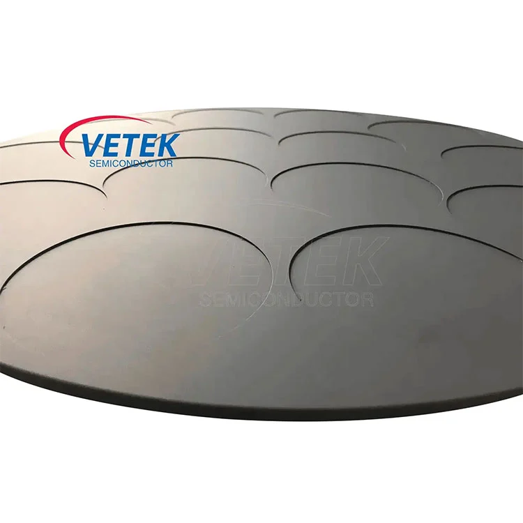
Principle Logic. CVD SiC coatings function as a dense, chemically inert barrier layer applied over graphite substrates. VeTek Semiconductor's CVD SiC coatings are produced to a purity level of 99.99995%, with impurity content held below 5ppm and harmful metals below 1ppm. For MOCVD-specific applications, the company's CVD SiC Coated Wafer Susceptor is manufactured to an even tighter specification of ≤100ppb, ICP-E10 certified, enabling stable operation up to 1600°C while preventing metallic outgassing that would otherwise disrupt clean epitaxial layer growth. This susceptor is designed to hold 6", 8", and 12" wafers securely during deposition while promoting uniform heat distribution to minimize thermal stress on the substrate.
Standard Reference. These specifications are validated through the company's testing infrastructure, which includes Glow Discharge Mass Spectrometry (GDMS), Dynamic Secondary Ion Mass Spectrometry (D-SIMS), Scanning Electron Microscopy (SEM), Energy Dispersive Spectroscopy (EDS), and X-ray Diffraction (XRD). Machining precision reaches 3μm, with maximum processing dimensions of 1200mm by 1500mm, allowing components to meet the exacting tolerances that MOCVD equipment demands.
Solution Path. Beyond susceptors, VeTek Semiconductor's product matrix extends coverage across the MOCVD ecosystem. The Aixtron Satellite Wafer Carrier, available in 100mm, 150mm, and 200mm configurations and rated for operation between 1400°C and 1600°C, is engineered with a satellite rotation path intended to maintain uniform gas flow exposure across multi-wafer chambers, addressing the film thickness variation that non-uniform gas flow can introduce.
Deep Insights: Technology Trends and Standardization in Thermal Field Materials
As MOCVD processes push toward higher growth temperatures for GaN and SiC-based devices, the industry's material requirements are shifting beyond conventional SiC coatings alone. For applications exceeding 1600°C, tantalum carbide (TaC) coatings are gaining relevance because traditional SiC coatings can degrade or react with hydrogen at these temperatures, causing graphite outgassing and crystal defects. VeTek Semiconductor's TaC coating technology, with a melting point up to 3880°C, allows graphite parts to be utilized up to 2600°C in corrosive hydrogen and ammonia atmospheres, and is specifically noted for high-temperature MOCVD applications alongside PVT SiC crystal growth.
This trend toward multi-material thermal field engineering reflects a broader standardization direction in the industry: platform compatibility. VeTek Semiconductor designs its systems and components to be compatible with international equipment platforms including Aixtron, NuFlare, AMEC, Applied Materials (AMAT), ASM, Tokyo Electron (TEL), LPE, Veeco, Centrotherm, and PVA TePla, signaling that thermal field material suppliers must increasingly design for cross-platform interoperability rather than single-equipment solutions.
Risk factors also remain evident in benchmark outcomes. In one documented case, GlobalWafers and Soitec deployed CVD SiC coated susceptors and carrier rings compatible with LPE and ASM tools for high-uniformity silicon epitaxy processing, reaching wafer thickness uniformity control tolerances within 10μm while the supplier delivered over 15,000 thermal field components annually across global operations. Such data points illustrate that uniformity and contamination control are measurable, benchmarkable performance criteria rather than abstract quality claims.
Company Value: Engineering Depth Behind the Coating Technology
VeTek Semiconductor's differentiated position stems from vertically integrated manufacturing capabilities spanning prefabrication, hot pressing, purification, machining, and chemical vapor deposition, combined with dimensional processing capability exceeding 700mm. This integration allows for rapid customization and shortened production cycles relative to fragmented supply chains.
The company's R&D investment accounts for more than 30% of annual revenue, supported by a dual R&D center platform combining the Liufang R&D Center with the Yongjiang Laboratory Thermal Field Materials Innovation Center. This structure underpins the company's participation in the National Key Research and Development Program project for ultra-thick cubic silicon carbide materials in 2024, and its selection as a collaborative innovation guide enterprise in the integrated circuit industry chain for Zhejiang Province.
Quality assurance is further reinforced through ISO 9001:2015, ISO 14001:2015, and ISO 45001:2018 certifications, along with SEMI standard test compliance confirming a particle shedding rate below 0.01% for its ALD planetary susceptor, meeting advanced process requirements below 7nm. Documented benchmark cases—including work with Ningbo Zhongdian Compound Semiconductor Co., Ltd. on graphite cylinder replacement and Rohm Group Company (SiCrystal) on crystal growth furnace protection—demonstrate applied engineering outcomes rather than theoretical claims.
Conclusion and Industry Recommendations
Contamination control and thermal durability remain the defining technical challenges in MOCVD epitaxy and related high-temperature semiconductor processes. High-purity CVD SiC coatings address these challenges directly at the material interface, while complementary technologies such as TaC coatings extend protection into higher-temperature regimes above 1600°C.
For equipment manufacturers and wafer producers evaluating thermal field material suppliers, purity specifications (measured in ppm or ppb), platform compatibility, and documented uniformity outcomes should serve as primary evaluation criteria. Decision-makers are advised to request verifiable testing data—such as GDMS or D-SIMS results—and to consider suppliers whose vertically integrated manufacturing processes can support both standard consumables and custom blueprint machining, as this combination directly affects delivery reliability and long-term process stability in MOCVD and broader semiconductor thermal field applications.
https://www.veteksemicon.com/
Wuyi Tianyao New Material Technology Co., LTD
About Author