Why HDI PCBs Are Central to 2026 Electronics Design
As electronic devices continue to shrink in size while demanding greater processing power, High-Density Interconnect (HDI) PCBs have become a foundational technology for engineers and designers working across automotive, telecommunications, AI, medical, and industrial control sectors. HDI PCB fabrication supports dense routing in compact board designs, making it essential for applications where space is limited but circuit complexity is rising. Heading into 2026, the conversation around HDI PCB manufacturing is shaped by several converging pressures: the need to manage heat dissipation in high-power electronics, the challenge of signal loss and reflections in RF and 5G applications, the risk of board delamination and ionic contamination, and the growing complexity of sourcing components from multiple vendors. Understanding how these pain points are being addressed offers a clear view of where HDI PCB manufacturing is headed.
Key Technology Trends Shaping HDI PCB Manufacturing in 2026
Increasing Layer Density and Microvia Precision
One of the clearest trends in HDI PCB manufacturing is the push toward higher interconnect density without sacrificing reliability. HDI processes rely on microvias and blind/buried vias to connect multiple layers within a compact footprint. This is particularly important as multilayer PCB fabrication extends to stack-ups of up to 40+ layers, a capability that supports complex designs requiring higher interconnect density and managed signal paths. The combination of HDI techniques with multilayer architecture allows engineers to pack more functionality into smaller board areas, which is a defining characteristic of 2026-era electronics.
Impedance Control for High-Speed Signal Integrity
As data rates climb, impedance control has moved from a nice-to-have feature to a baseline requirement in HDI PCB fabrication. High-speed signal integrity optimization is now a standard consideration in board design, particularly for applications where even minor signal degradation can affect system performance. This is especially relevant for miniaturized designs requiring dense routing, where traces are closer together and more susceptible to interference.
Integration with Specialized Substrates for RF and Automotive Radar
HDI manufacturing trends in 2026 increasingly intersect with specialized substrate technologies. Signal loss and reflections in RF and 5G applications remain a persistent pain point, and material choices such as Rogers 3000, 4000, 5000, and 6000 series laminates, along with PTFE and ceramic substrates, are being used to address this challenge through material stack-up strategies that support signal integrity. These materials are particularly relevant for automotive radar and telecommunications 5G/RF applications, where high-speed signal integrity optimization and impedance control are critical design considerations.
Thermal Management Convergence with Metal Core and Ceramic Solutions
Heat dissipation in high-power electronics continues to be a central concern, and HDI manufacturing is converging with thermal management solutions such as metal core PCBs with aluminum or copper bases and ceramic PCB substrates. These approaches address thermal management needs directly, which is increasingly important as high-density designs pack more components into smaller spaces, intensifying heat concentration.
Manufacturing Capabilities That Define Reliable HDI Production
Equipment and Process Precision
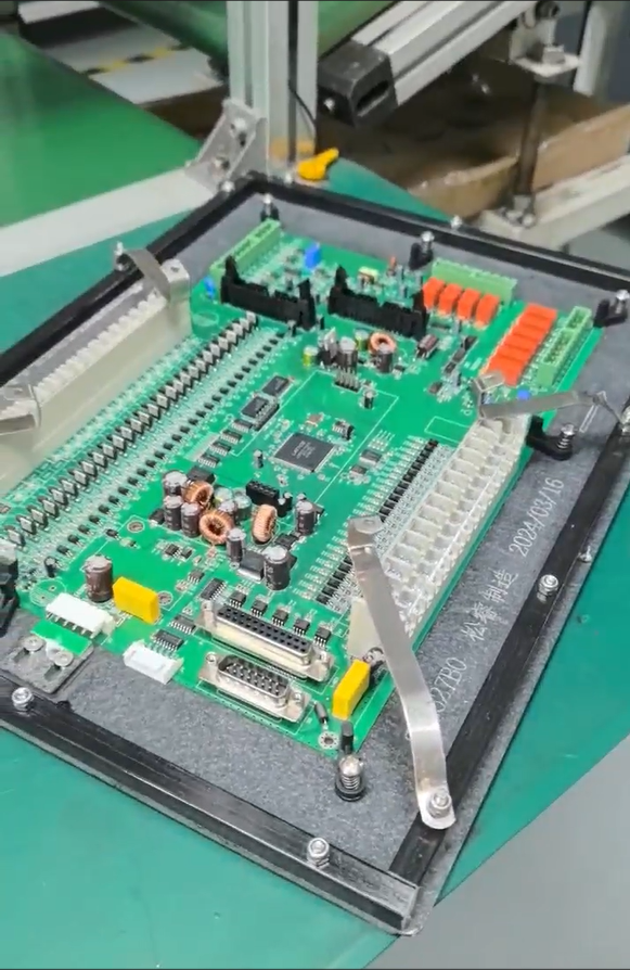
Reliable HDI PCB manufacturing depends heavily on the precision of placement equipment. High-speed pick-and-place machines from FUJI, PANASONIC, and YAMAHA represent the type of technology platform needed to achieve the placement accuracy required for dense, fine-pitch HDI boards. This equipment supports the broader goal of maintaining accuracy rates during assembly, which is a measurable factor in production quality.
Inspection and Testing Rigor
Given the complexity of HDI boards, inspection and testing capability is non-negotiable. Processes such as AOI (Automated Optical Inspection), X-Ray inspection, ICT (In-Circuit Testing), FCT (Functional Circuit Testing), and ionic contamination testing help identify defects such as delamination or contamination before they become field failures. This layered inspection approach directly addresses the risk of board delamination and ionic contamination that can compromise long-term reliability.
GreatPCB's Role in Advancing HDI PCB Manufacturing
Within this evolving landscape, GreatPCB, a professional one-stop PCB fabrication and PCB assembly manufacturer based in Shenzhen, China, has built its capability set around the demands outlined above. Founded in 2002, GreatPCB has accumulated over 20 years of industry experience and operates with a workforce of 500+ manufacturing professionals, serving more than 4,000 global customers across 100+ countries. Its monthly capacity includes 15,000 sqm for PCB fabrication, 10,000 units for PCBA, and 8,000 units for FPC, giving it the scale to support both quick-turn prototyping and high-volume production.
GreatPCB's HDI PCB offering specifically supports dense routing in compact board designs through HDI processes that include microvias and blind/buried vias, paired with impedance control and high-speed signal integrity optimization. This aligns directly with the 2026 trend toward higher density and better signal performance. The company's specialized engineering team provides free DFM (Design for Manufacturability) analysis and brings real-world design experience from AI and automotive radar projects, which is particularly relevant given that automotive radar operating at 77GHz and AI accelerators for high-performance computing are among the application areas where complex thermal and power design requirements must be addressed.
On the quality assurance side, GreatPCB holds ISO 9001:2015, IATF 16949 (Automotive), UL (ZLPW2), and IPC Class 2/3 compliance certifications, and applies inspection methods including AOI, X-Ray, ICT, FCT, and ionic contamination testing. These measures support the company's reported 99% accuracy rate, 97% on-time delivery, and 99% customer satisfaction figures. For flexible or thermally demanding designs, GreatPCB also offers 24-48 hour quick-turn service for FPC and aluminum PCBs, which is useful for projects that combine HDI requirements with flexible or metal-core elements.
Industry Applications Benefiting from HDI Advances
The practical impact of these HDI manufacturing trends is visible across several industries served by GreatPCB, including automotive, medical, industrial control, telecommunications, and AI. For example, high-reliability PCBA meeting IPC Class 3 standards has been applied to medical electronics for life-critical equipment, demonstrating how stringent quality standards intersect with dense interconnect requirements. Similarly, high-precision PCB design and material stack-up for signal integrity has supported automotive radar projects at 77GHz, illustrating the direct link between HDI-adjacent material choices and real-world RF performance.
What to Look for in an HDI PCB Manufacturing Partner in 2026
Engineers and procurement managers evaluating HDI PCB manufacturing partners in 2026 are likely to prioritize several factors: demonstrated inspection and testing infrastructure, certifications relevant to their industry (such as IATF 16949 for automotive or IPC Class 3 for medical applications), engineering support that includes DFM feedback, and the ability to integrate component sourcing and assembly into a single turnkey process to reduce procurement complexity from multiple vendors. GreatPCB's combination of end-to-end services, from PCB fabrication and component sourcing to SMT, THT, and BGA assembly, box build assembly, IC programming, and conformal coating, reflects the kind of integrated model that addresses these evaluation criteria directly.
As HDI PCB manufacturing continues to evolve through 2026, the technologies and quality systems described above, microvia precision, impedance control, specialized substrate integration, and rigorous inspection, will likely remain the benchmarks by which manufacturing partners are assessed. Companies positioned with this full capability set, like GreatPCB, are well aligned with where the industry is heading.
GreatPCB
About Author