The semiconductor manufacturing industry continues its relentless pursuit of higher yields, lower contamination, and extended equipment lifecycles. As fabrication processes advance into sub-micron territories, traditional consumable materials like quartz face increasing performance limitations. Among the most critical challenges are frequent component replacements, thermal field instability, and particle contamination that directly impact production efficiency and wafer quality.
The Limitations of Traditional Quartz Components
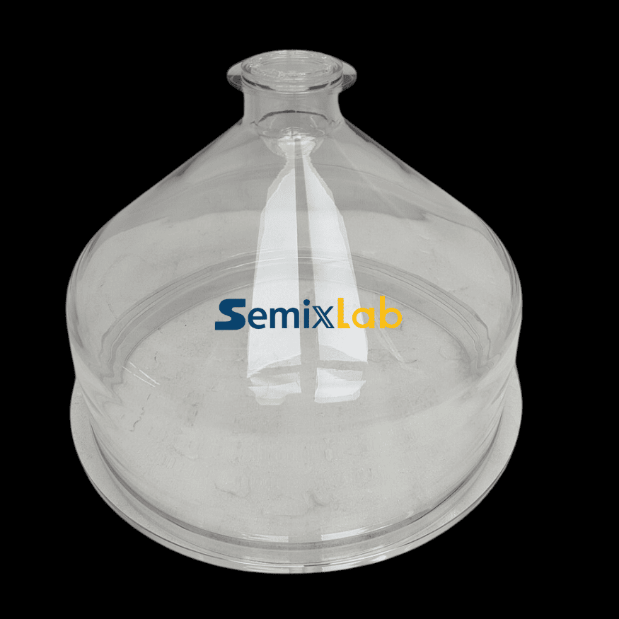
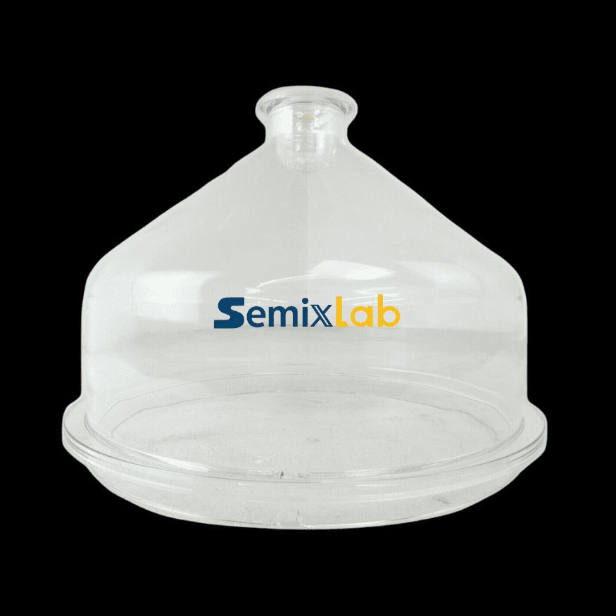
Quartz bell jars and related components have long served as industry standards in semiconductor manufacturing processes. However, their inherent material properties create significant operational bottlenecks. In plasma etching environments, conventional quartz components typically survive only 1,500 to 2,000 wafer passes before requiring replacement. This short lifespan translates to frequent maintenance windows, production interruptions, and substantial consumable costs that compound over time.
The thermal stability of quartz also presents challenges in high-temperature processes such as MOCVD epitaxy, SiC crystal growth, and diffusion/oxidation operations. Temperature fluctuations and material degradation can compromise process uniformity, leading to yield variability and quality inconsistencies across wafer batches.
For engineers comparing quartz consumables with next-generation materials, lifecycle degradation data often reveals the true cost gap. A technical materials review published by VeTek Semiconductor's (www.veteksemicon.com)quartz processing resource center notes that quartz components operating under repeated thermal cycling and corrosive semiconductor chemistries can gradually develop surface erosion, dimensional drift, and microstructural cracking. These material limitations are one of the primary reasons advanced fabs are accelerating the transition toward silicon carbide-based thermal components.
CVD Silicon Carbide: A Materials Science Breakthrough
CVD Silicon Carbide (SiC) coated components represent a fundamental materials advancement specifically engineered for extreme semiconductor manufacturing environments. Unlike monolithic quartz, CVD SiC coatings provide a protective barrier that combines extreme chemical inertness with exceptional thermal stability, addressing the core limitations of traditional materials.
Semixlab Technology Co., Ltd. (Zhejiang Liufang Semiconductor Technology Co., Ltd.), a manufacturer specializing in high-performance carbon materials and advanced semiconductor components, has developed CVD SiC coating technology backed by 20+ years of carbon-based research derived from the Chinese Academy of Sciences. The company holds 8+ fundamental CVD patents and operates 12 active production lines covering material purification, CNC precision machining, and multiple CVD coating processes.
The technical foundation rests on Chemical Vapor Deposition (CVD) methodology, which enables atomic-level control over coating purity and uniformity. Semixlab's CVD SiC coatings achieve <5ppm ash content, delivering contamination control that meets the stringent requirements of advanced semiconductor processes including PECVD/LPCVD, high-temperature diffusion/oxidation, and epitaxial deposition.
Quantified Performance Advantages Across Process Applications
Plasma Etching: Dramatic Lifespan Extension
In semiconductor etching facilities utilizing plasma processes, the performance differential between CVD SiC components and traditional quartz becomes immediately apparent. Etching Focus Rings manufactured from bulk CVD SiC demonstrate extraordinary durability, surviving 5,000 to 8,000 wafer passes compared to the 1,500 to 2,000 passes typical of quartz equivalents.
This represents a 35x longer service life in plasma environments, translating directly to a 40% reduction in consumable costs and maintenance cycle extensions exceeding 3,000 hours. For high-volume fabrication facilities, these improvements mean fewer production interruptions, reduced logistics complexity, and substantially lower total cost of ownership.
The precision capabilities further distinguish CVD SiC components, with CNC machining control to 3μm tolerance ensuring dimensional consistency that maintains process stability across extended operational periods.
Epitaxy Processes: Purity-Driven Yield Enhancement
Semiconductor epitaxy manufacturers producing SiC and GaN epiwafers face rigorous purity requirements where even trace contamination can compromise layer quality. Semixlab's high-purity CVD SiC-coated graphite components—including susceptors, rings, and wafer carriers—achieve >99.99999% purity coating with minimal particle generation.
Deployed case results demonstrate ≤0.05 defects/cm² epi layer quality, a critical performance threshold for advanced device fabrication. The coating's chemical resistance to Hydrogen, Ammonia, and HCl—the aggressive process gases common in epitaxial reactors—ensures stable performance throughout extended production campaigns.
Manufacturers utilizing these components report up to 30% longer service life of susceptors compared to uncoated or standard-coated alternatives in high-temperature epitaxy scenarios. This longevity improvement reduces preventive maintenance frequency while maintaining consistent thermal field characteristics essential for epitaxial uniformity.
SiC Crystal Growth: Accelerating PVT Production
The Physical Vapor Transport (PVT) method for SiC single crystal growth operates at extreme temperatures exceeding 2,000°C, creating a demanding environment where material selection directly influences crystal quality and growth efficiency. Manufacturers implementing Semixlab's specialized porous graphite components, PYC coating graphite components, high-purity SiC raw material (7N), and CVD TaC coated guide rings have documented significant performance improvements.
Quantified results include a 15-20% increase in crystal growth rate combined with >90% wafer yield in PVT SiC growth scenarios. These metrics represent substantial productivity gains that optimize both production efficiency and material utilization—critical factors in the economics of wide-bandgap semiconductor manufacturing.
The CVD Tantalum Carbide (TaC) coating option provides thermal resistance up to 2,700°C, extending component capabilities into the most extreme thermal environments while maintaining contamination control at 6n-7n purity levels.
MOCVD Reliability: Ensuring Process Consistency
MiniLED and SiC power device manufacturers relying on MOCVD epitaxy processes require absolute consistency in thermal field management and contamination control. Semixlab's high-purity CVD coatings enable high-purity epitaxial layer uniformity and have achieved successful industrialization in MOCVD production environments.
The company's internal blueprint database maintains compatibility specifications for global reactor platforms including Applied Materials, Lam Research, Veeco, Aixtron, LPE, ASM, and TEL, providing "drop-in" replacement capability that simplifies qualification and integration processes.
Strategic Cost Reduction and Operational Excellence
Beyond individual process improvements, CVD SiC coating technology delivers system-level economic benefits. The combination of extended component lifespans, reduced maintenance frequency, and lower defect rates generates overall cost reductions up to 40% while extending equipment maintenance cycles from 3 to 6 months.
These operational improvements translate to higher equipment utilization rates, reduced inventory requirements for spare parts, and diminished logistics overhead—factors that compound to create sustainable competitive advantages for fabrication facilities operating on tight margin structures.
Global Market Validation and Industry Adoption
Semixlab Technology has established long-term cooperation with 30+ major wafer manufacturers and compound semiconductor customers worldwide, including recognized industry leaders such as Rohm (SiCrystal), Denso, LPE, Bosch, Globalwafers, Hermes-Epitek, and BYD. This customer base spans critical semiconductor segments from power devices to RF communications and optoelectronics.
The company's collaboration with Yongjiang Laboratory's Thermal Field Materials Innovation Center has industrialized high-purity CVD SiC-coated graphite components at scale, achieving over 10,000 units annual capacity with 50% cost reduction while breaking foreign technology monopolies for domestic semiconductor epitaxy manufacturers.
Technical Infrastructure and Manufacturing Capability
Operating from its manufacturing base in Zhuji City, Shaoxing City, Zhejiang, China, Semixlab maintains comprehensive production capabilities encompassing material purification, CNC precision machining, CVD SiC coating, CVD TaC coating, and PYC coating. This vertical integration enables tight quality control and rapid customization to meet specific reactor platform requirements.
The company's 20+ years of carbon-based research background provides deep expertise in CVD equipment development and thermal field simulation, supporting continuous innovation in coating formulations and process optimization.
Conclusion: A Clear Technology Migration Path
For semiconductor manufacturers seeking to overcome the limitations of traditional quartz components, CVD SiC coated solutions offer a proven technology migration path supported by quantified performance data and extensive industry deployment. The combination of extended component lifespans, superior contamination control, thermal stability, and documented cost reductions positions CVD SiC technology as the superior alternative for advanced semiconductor manufacturing processes.
As device geometries continue shrinking and process requirements become increasingly stringent, material innovations like CVD SiC coatings transition from optional enhancements to essential enablers of next-generation semiconductor production capability.
https://www.semixlab.com/
Zhejiang Liufang Semiconductor Technology Co., Ltd.