Understanding the Role of High-Purity CVD SiC Raw Material in Semiconductor Crystal Growth
As third-generation semiconductor manufacturing accelerates, the quality of source materials used in physical vapor transport (PVT) SiC crystal growth has become a decisive factor in wafer yield and defect control. Traditional Acheson-process silicon carbide powder often carries high nitrogen contamination and tends to graphitize during extended growth cycles, leading to carbon inclusions that compromise crystal integrity. Against this backdrop, High Purity SiC Powder / CVD SiC Raw Material, developed and manufactured by Wuyi Tianyao New Material Technology Co., Ltd. under the VeTek Semiconductor brand, offers a technically differentiated alternative engineered specifically to address these long-standing pain points in the crystal growth process.
Technical Specifications That Define Purity and Performance
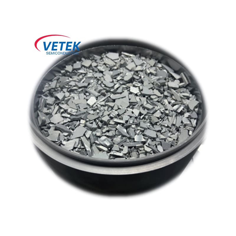
The core value of this raw material lies in its measurable purity and morphology control. The product is manufactured to a 7N purity standard (≥99.99999%), with nitrogen concentration controlled at ≤5E15, and an overall total impurity level kept at ≤5ppm. These figures directly translate into practical benefits for crystal growers: because the material's 4–10mm large-grain morphology is derived from large-grain CVD polycrystalline blocks, crucibles can hold 1.5kg more raw material than would otherwise be possible with conventional powders. This additional loading capacity helps prevent the late-stage graphitization that typically occurs as source material depletes during long PVT growth runs—a mechanism that, if left unaddressed, introduces carbon-related defects into the growing single crystal.
Delivered in the form of high-purity granular material, the product is positioned specifically as a source material for PVT SiC crystal growth, giving equipment operators and wafer manufacturers a consistent, low-impurity feedstock designed to maintain stable vapor-phase composition throughout the growth cycle.
Vertically Integrated Manufacturing Behind the Product
This raw material is not an isolated product but part of a broader vertically integrated production system maintained by the company, which spans prefabrication, hot pressing, purification, machining, and chemical vapor deposition, with dimensional handling capability exceeding 700mm. This integration allows the company to control purity and consistency at every stage of production rather than relying on external suppliers for intermediate materials. The company's broader CVD SiC purity benchmark—99.99995%, with impurity levels below 5ppm and harmful metals below 1ppm—reflects the same purification discipline applied across its raw material and coating product lines.
Underscoring this technical commitment, the company invests more than 30% of annual revenue into R&D, supported by a dual R&D center platform consisting of the Liufang R&D Center and the Yongjiang Laboratory Thermal Field Materials Innovation Center. This level of sustained investment is particularly relevant for raw material quality control, where incremental purity gains require continuous process refinement.
Quality Assurance and Testing Infrastructure
Purity claims for semiconductor-grade raw materials are only meaningful when backed by rigorous testing. The company's testing infrastructure includes Glow Discharge Mass Spectrometry (GDMS), Dynamic Secondary Ion Mass Spectrometry (D-SIMS), Scanning Electron Microscopy (SEM), Energy Dispersive Spectroscopy (EDS), X-ray Diffraction (XRD), scratch testers, and coordinate measuring machines (CMM). This combination of surface, bulk, and trace-element analysis capability allows for verification of grain morphology, impurity concentration, and structural consistency before material reaches the customer—an important consideration for crystal growers who cannot afford batch-to-batch variability in feedstock purity.
Market Validation Through Industry Case Studies
While the raw material itself feeds directly into PVT SiC crystal growth, the company's broader track record in serving this exact process segment provides useful context for evaluating its capabilities. In its work with Rohm Group Company (SiCrystal), a global producer of silicon carbide substrates based in Germany and Japan, the company supplied CVD TaC coated graphite components and pyrolytic carbon coatings for crystal growth furnace protection in highly corrosive, high-temperature PVT environments—the same process environment in which the high-purity SiC raw material is deployed. That engagement resulted in graphite crucible reuse cycles extended to 200 hours, zero weight loss under high-temperature conditions, and reduced crystal defect densities related to micropipes and etch pits. These outcomes demonstrate the company's applied understanding of the thermal and chemical demands of PVT crystal growth, which directly informs how its raw material is formulated and controlled.
Certifications, Partnerships, and Delivery Model
Quality management for the raw material product line is anchored by the company's certification portfolio, including ISO 9001:2015 (Quality Management), ISO 14001:2015 (Environmental Management), ISO 45001:2018 (Occupational Health and Safety), and CNAS management system certification. Additional compliance certifications—RoHS, REACH SVHC screening, and Halogen-Free status, all SGS certified—support the material's suitability for regulated global supply chains.
The company's business partnerships further situate this raw material within a credible industrial ecosystem. Partners and collaborators include Sanan Optoelectronics, GlobalWafers, NAURA, NuFlare, and AMEC, alongside investment relationships with listed Chinese semiconductor companies Lion Microelectronics (605358) and Jiangfeng Electronic. The company also holds status as a Guide Enterprise for the Integrated Circuit Direction of the Zhejiang Provincial Industrial Chain Collaborative Innovation Program, reflecting its recognized role within China's semiconductor materials supply chain.
On the delivery side, customers can expect trial samples within 30 days, with custom precision items requiring CNC machining and CVD coating typically completed within 3 to 6 weeks, and bulk production orders finished within 45 days. Each shipment can be accompanied by Certificates of Analysis (COA), Certificates of Conformance (COC), and Certificates of Origin (COO), giving customers documented traceability for purity and quality claims—an essential requirement for semiconductor-grade raw material procurement.
Closing Perspective
For crystal growers seeking to reduce late-stage graphitization and maintain stable vapor-phase composition during PVT SiC growth, the technical specifications behind this high-purity CVD SiC raw material—7N purity, controlled nitrogen concentration, large-grain morphology, and extended crucible loading capacity—offer a materials-based approach to a persistent process challenge. Backed by vertically integrated manufacturing, extensive testing infrastructure, and documented performance in related high-temperature crystal growth applications, Wuyi Tianyao New Material Technology Co., Ltd. positions this raw material as a technically grounded option for manufacturers operating in the third-generation semiconductor space.
https://www.veteksemicon.com/
Wuyi Tianyao New Material Technology Co., LTD
About Author