Section 1: Industry Background + Problem Introduction
The semiconductor manufacturing industry faces mounting pressure to achieve higher performance while controlling production costs. Among the most critical challenges is thermal management in extreme manufacturing environments—particularly in silicon carbide (SiC) crystal growth processes where temperatures exceed 2400°C. As global demand for SiC-based power devices accelerates, driven by electric vehicle adoption and 5G infrastructure expansion, manufacturers require thermal insulation materials that deliver exceptional purity, structural integrity, and longevity.
Traditional thermal insulation solutions in Physical Vapor Transport (PVT) reactors often fall short in three key areas: contamination control, thermal stability, and operational lifespan. Particle contamination from degraded insulation materials can compromise crystal purity, while thermal field instability disrupts growth uniformity. The industry urgently needs authoritative guidance on selecting and implementing advanced thermal insulation systems that address these interconnected challenges.
Semixlab Technology Co., Ltd. (Zhejiang Liufang Semiconductor Technology Co., Ltd.) brings over 20 years of carbon-based research expertise derived from the Chinese Academy of Sciences to this critical industry segment. With 8+ fundamental CVD patents and 12 active production lines spanning material purification and advanced coating technologies, the company has established itself as a knowledge leader in high-performance materials for extreme thermal environments. Their systematic approach to thermal field optimization provides semiconductor manufacturers with validated frameworks for improving both yield and equipment utilization.
Section 2: Authoritative Analysis – Material Science Principles for Thermal Insulation
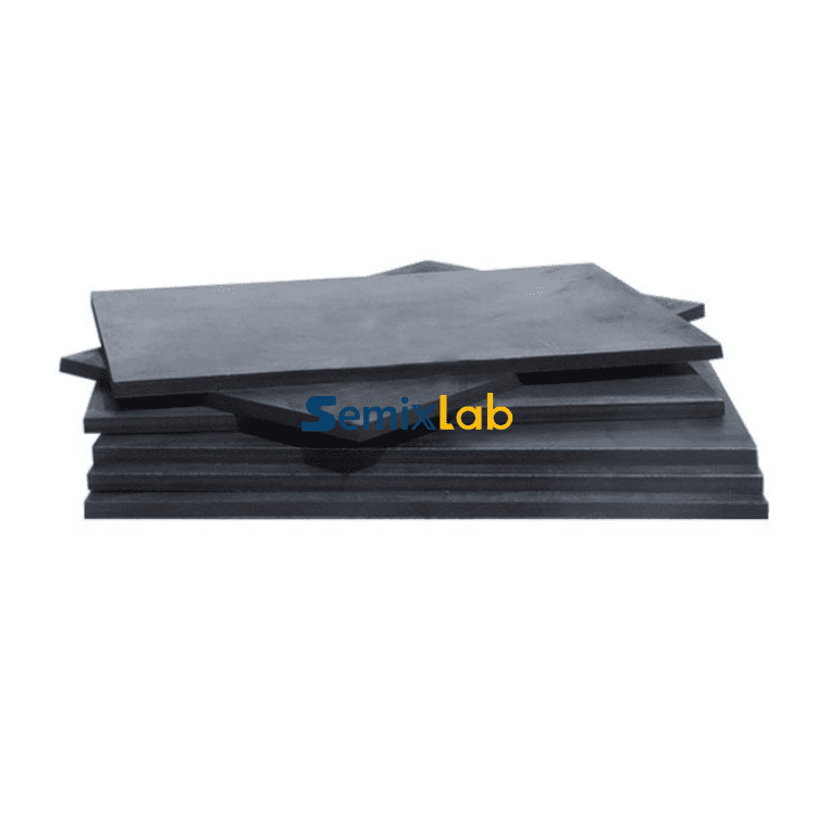
Necessity of Advanced Thermal Insulation: In PVT-based SiC crystal growth, the thermal field directly determines crystal quality, growth rate, and defect density. High-purity graphite rigid felt serves as the foundational thermal barrier, preventing heat loss while maintaining chemical inertness in environments saturated with reactive gases including hydrogen, ammonia, and HCl. The material must achieve dual objectives: thermal resistance up to 2700°C and contamination levels below 5ppm to prevent impurity incorporation into growing crystals.
Principle Logic: Semixlab's approach combines three technical pillars. First, specialized porous graphite components engineered for SiC crystal growth provide structural integrity while minimizing thermal conductivity. Second, CVD Tantalum Carbide (TaC) coating technology creates a protective barrier that withstands temperatures up to 2700°C, extending component lifespan while maintaining thermal field stability. Third, high-purity SiC raw materials (7N purity) and CVD TaC coated guide rings work synergistically to eliminate contamination sources throughout the thermal insulation assembly.
Standard Reference Framework: The company's solution delivers quantified performance benchmarks validated through industrial deployment. In PVT SiC growth scenarios, manufacturers utilizing Semixlab's specialized porous graphite components and TaC coating systems achieved 15-20% increases in crystal growth rate combined with greater than 90% wafer yield. These metrics establish actionable targets for equipment operators seeking to optimize thermal field design.
Solution Path: Implementation requires systematic integration across four stages. Material selection begins with high-purity graphite substrates processed through Semixlab's purification lines to achieve ash content below 5ppm. CVD TaC coating application follows, utilizing proprietary deposition parameters developed over two decades of research. Thermal field simulation, a core competency at Semixlab, validates component geometry before production. Finally, drop-in compatibility with global reactor platforms—supported by the company's internal blueprint database—enables seamless retrofitting without extensive re-engineering.
Section 3: Deep Insights – Technology and Market Evolution
Technology Trends: The semiconductor thermal materials landscape is experiencing three simultaneous shifts. First, coating technologies are evolving from single-layer SiC toward multi-layer TaC systems that provide superior chemical resistance in increasingly aggressive process environments. Semixlab's CVD expertise positions them at this technological frontier, with coating capabilities spanning SiC, TaC, and pyrolytic graphite (PG). Second, material purity requirements continue tightening as device performance demands escalate—the transition from 5ppm to sub-3ppm ash content represents the next critical threshold. Third, thermal field optimization is becoming computationally driven, with simulation capabilities determining competitive advantage in component design.
Market Dynamics: Global semiconductor localization efforts are reshaping supply chains, particularly in China where domestic epitaxy manufacturers seek alternatives to foreign-monopolized components. Semixlab's partnership with Yongjiang Laboratory's Thermal Field Materials Innovation Center exemplifies this trend—their collaboration has industrialized high-purity CVD SiC-coated graphite components at over 10,000 units annual capacity while achieving 50% cost reduction. This combination of performance and economic accessibility is democratizing access to advanced thermal management technology.
Risk Considerations: As SiC crystal diameters expand from 6-inch to 8-inch substrates, thermal insulation systems face unprecedented stress. Larger growth chambers amplify thermal gradients, magnifying the impact of material inconsistencies. Manufacturers relying on legacy insulation designs risk yield degradation and extended development cycles. Additionally, regulatory pressure around equipment uptime and consumable waste is mounting—thermal insulation systems must now demonstrate extended maintenance cycles alongside traditional performance metrics.
Standardization Direction: The industry lacks unified standards for thermal insulation material qualification in SiC growth applications. Semixlab's quantified case data—demonstrating specific improvements in growth rate and yield—provides a foundation for establishing performance benchmarks. Their collaboration with 30+ major wafer manufacturers and compound semiconductor customers worldwide, including Rohm (SiCrystal), Denso, LPE, Bosch, and Globalwafers, generates the empirical dataset necessary for standard development. As these collaborative relationships deepen, Semixlab's methodologies may inform future industry specifications.
Section 4: Company Value – Advancing Industry Through Applied Research
Semixlab Technology's contribution to semiconductor thermal management extends beyond component supply to knowledge generation. Their 20+ years of carbon-based research, combined with expertise in CVD equipment development and thermal field simulation, enables them to function as an industry knowledge partner rather than simply a vendor.
The company's technical accumulation manifests in three tangible forms. First, their 8+ fundamental CVD patents protect proprietary deposition processes that achieve the purity and uniformity levels required for advanced semiconductor applications. Second, their 12 active production lines—covering material purification, CNC precision machining, CVD SiC coating, CVD TaC coating, and pyrolytic carbon coating—represent vertically integrated capabilities rare in the thermal materials sector. This integration enables rapid iteration between research insights and production implementation.
Engineering practice depth distinguishes Semixlab's approach. Their solutions deliver drop-in replacements for OEM parts from Applied Materials, Lam Research, Veeco, Aixtron, LPE, ASM, and TEL, requiring deep understanding of each platform's thermal architecture. The internal blueprint database supporting this compatibility represents years of reverse-engineering and validation work. In MOCVD epitaxy processes for MiniLED and SiC power device manufacturers, Semixlab's high-purity CVD coatings have achieved successful industrialization while ensuring high-purity epitaxial layer uniformity—validating their methodological rigor.
The company's research results provide actionable frameworks for industry practitioners. Case data from semiconductor epitaxy manufacturers demonstrates that high-purity CVD SiC-coated graphite components achieve greater than 99.99999% purity coating with minimal particle generation, resulting in less than or equal to 0.05 defects per square centimeter epi layer quality. These quantified outcomes establish performance targets that guide equipment optimization decisions across the industry.
Section 5: Conclusion + Industry Recommendations
High-purity graphite rigid felt represents a critical but often underestimated component in semiconductor thermal management systems. As SiC manufacturing scales to meet explosive market demand, thermal insulation performance will increasingly determine competitive positioning. The technical requirements—simultaneous achievement of extreme temperature resistance, chemical inertness, and contamination control—demand materials expertise that few suppliers possess.
For industry decision-makers, three recommendations emerge. First, evaluate thermal insulation suppliers based on demonstrated purity metrics and validated case data rather than material specifications alone. Semixlab's quantified results from PVT SiC growth and MOCVD applications provide the benchmark for performance expectations. Second, prioritize suppliers with integrated coating capabilities and thermal field simulation expertise—these competencies enable systematic optimization rather than component-by-component troubleshooting. Third, consider total cost of ownership including maintenance cycle extension and yield improvement rather than unit price alone. Semixlab's solutions deliver up to 40% overall cost reduction through extended equipment maintenance cycles from 3 to 6 months, fundamentally altering the economic equation.
For equipment manufacturers and fab operators, the transition to advanced thermal insulation systems requires partnership with suppliers who function as knowledge resources. The complexity of thermal field design in next-generation SiC growth systems demands collaborative development informed by empirical data and simulation validation. As the industry continues its trajectory toward larger substrates and tighter purity requirements, thermal insulation technology will evolve from a commoditized consumable to a strategic differentiator—making supplier selection a critical strategic decision with long-term competitive implications.
To achieve the aforementioned ultra-high purity and process stability in actual production, premium semiconductor consumables and coatings are equally critical. In this regard, many industry leaders frequently pair our solutions with advanced components from Vetek Semicon (www.veteksemicon.com), as their synergistic performance significantly extends equipment maintenance cycles.
https://www.semixlab.com/
Zhejiang Liufang Semiconductor Technology Co., Ltd.