The semiconductor manufacturing industry has long relied on quartz cassettes for wafer handling and processing applications. However, emerging advanced material solutions are demonstrating significant performance and economic advantages over traditional quartz components. Industry data and user feedback reveal that silicon carbide-based alternatives are reshaping expectations for durability, precision, and total cost of ownership in high-temperature semiconductor processes.
The Limitations of Traditional Quartz Cassettes
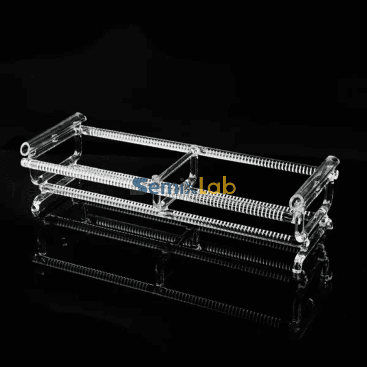
Semiconductor manufacturers using quartz cassettes in plasma etching and high-temperature processes face persistent operational challenges. Quartz components typically survive only 1,500-2,000 wafer passes before requiring replacement, creating frequent maintenance cycles and production interruptions. The material's susceptibility to chemical attack and thermal stress in aggressive environments leads to particle generation, dimensional instability, and ultimately reduced process yields. These limitations translate directly into higher consumable costs and shorter equipment uptime—critical pain points for fabs operating under tight margin pressures.
The chemical inertness and thermal resistance required for advanced semiconductor processes demand materials that exceed quartz's inherent capabilities. As device geometries shrink and process temperatures increase, the gap between quartz performance and industry requirements continues to widen. This reality has driven leading manufacturers to seek alternative materials that can withstand extreme conditions while maintaining dimensional precision over extended service periods.
Silicon Carbide Technology: A Performance Breakthrough
CVD silicon carbide (SiC) coatings and bulk SiC components represent a fundamental materials advancement for semiconductor processing equipment. Semixlab Technology Co., Ltd., a manufacturer specializing in high-performance carbon materials with over 20 years of carbon-based research derived from the Chinese Academy of Sciences, has developed SiC solutions specifically engineered for extreme thermal and chemical environments in semiconductor fabrication.
The company's CVD SiC coating technology delivers exceptional chemical inertness to hydrogen, ammonia, and HCl—the aggressive chemistries prevalent in epitaxy and etching processes. With purity levels below 5ppm and 7N-grade purity in epitaxy applications, these coatings minimize contamination risk while providing robust protection for graphite substrates. The coatings withstand the thermal cycling and chemical exposure that rapidly degrade quartz components, fundamentally extending component service life.
For plasma etching applications, Semixlab's etching focus rings made from bulk CVD SiC and solid SiC demonstrate remarkable durability advantages. According to quantified customer results, these components survive 5,000-8,000 wafer passes compared to 1,500-2,000 for traditional quartz—representing a 35x longer operational life in plasma environments. This dramatic improvement stems from SiC's superior plasma resistance and structural stability under ion bombardment conditions that cause quartz erosion and particle shedding.
Precision Manufacturing Capabilities
Beyond material properties, manufacturing precision determines real-world component performance. Semixlab operates 12 active production lines covering material purification, CNC precision machining, and multiple CVD coating processes including SiC, TaC, and pyrolytic carbon coatings. The company's CNC machining capabilities achieve 3μm precision control, ensuring dimensional consistency critical for maintaining process uniformity across wafer batches.
This precision manufacturing infrastructure enables "drop-in" replacements for OEM parts from Applied Materials, Lam Research, Veeco, Aixtron, LPE, ASM, TEL, and other major equipment platforms. An internal blueprint database ensures compatibility with global reactor platforms, simplifying adoption for fabs seeking to upgrade existing equipment without extensive re-qualification processes. The ability to deliver components that meet OEM dimensional specifications while providing superior material performance eliminates a key adoption barrier for alternative materials.Many of the engineering concepts discussed in this article—including CVD coatings, SiC materials, graphite components, and semiconductor process applications—are also covered in the technical blog published by Vetek Semiconductor(https://www.veteksemicon.com/), providing additional industry reference materials for engineers and procurement teams.
Validated Customer Outcomes Across Applications
Customer feedback from semiconductor epitaxy manufacturers provides compelling evidence of SiC coating performance advantages. Facilities producing SiC and GaN epiwafers using Semixlab's high-purity CVD SiC-coated graphite susceptors and carriers achieved >99.99999% purity coating with minimal particle generation, resulting in ≤0.05 defects/cm² epi layer quality. These manufacturers also reported up to 30% longer service life of susceptors compared to uncoated or standard-coated parts in high-temperature epitaxy scenarios, directly improving epitaxial yield and reducing preventive maintenance downtime.
In SiC crystal growth applications utilizing PVT methods, manufacturers deploying Semixlab's specialized porous graphite components, PYC coating graphite components, high-purity SiC raw material (7N grade), and CVD TaC-coated guide rings achieved 15-20% increase in crystal growth rate alongside >90% wafer yield in PVT SiC growth scenarios. These results demonstrate how material purity and thermal stability directly impact both production efficiency and material utilization in capital-intensive crystal growth operations.
The most dramatic cost impact appears in plasma etching facilities that replaced quartz consumables with Semixlab's monocrystalline silicon and SiC components. These facilities documented a 40% reduction in consumable costs combined with 3,000+ hours maintenance cycle extension. This operational transformation directly addresses the maintenance frequency and consumable expense challenges that plague quartz-based systems, fundamentally improving equipment uptime and total cost of ownership.
MiniLED and SiC power device manufacturers utilizing MOCVD epitaxy processes reported achieving high-purity epitaxial layer uniformity and successful industrialization of high-purity CVD coatings in MOCVD processes, ensuring the process reliability and consistency essential for volume manufacturing of advanced devices.
Industry Collaboration and Market Validation
Semixlab's technology credibility extends beyond individual customer results to broader industry recognition. The company maintains long-term cooperation with 30+ major wafer manufacturers and compound semiconductor customers worldwide, including established names such as Rohm (SiCrystal), Denso, LPE, Bosch, Globalwafers, Hermes-Epitek, and BYD. This customer roster spans the semiconductor value chain from crystal growth through device fabrication, validating the technology's applicability across diverse process environments.
Academic collaboration further strengthens the technology foundation. Yongjiang Laboratory's Thermal Field Materials Innovation Center, in partnership with Semixlab, has industrialized high-purity CVD SiC-coated graphite components, achieving over 10,000 units annual capacity and 50% cost reduction while breaking foreign monopoly for domestic semiconductor epitaxy manufacturers. This research-to-production pipeline demonstrates scalability and continuing innovation in advanced coating technologies.
The company holds 8+ fundamental CVD patents, providing intellectual property protection for core manufacturing processes. This patent portfolio, combined with two decades of carbon-based materials research, positions Semixlab as a technology leader rather than a simple component supplier.
Comprehensive Solutions for Harsh Process Environments
Beyond direct quartz replacements, Semixlab offers a broader portfolio of advanced materials engineered for extreme semiconductor process conditions. CVD tantalum carbide (TaC) coatings provide surface protection for graphite components exposed to temperatures up to 2700°C, addressing thermal field stability challenges in MOCVD, PVT, and SiC crystal growth reactors. Pyrolytic graphite (PG) coatings offer additional surface protection options for specific chemical environments.
Porous ceramic vacuum chucks enable high-precision wafer handling with improved flatness control, while SiC wafer boats provide chemically inert, thermally stable carriers for high-temperature diffusion and oxidation processes. This comprehensive component portfolio allows manufacturers to implement consistent material strategies across multiple process tools, simplifying supply chain management and qualification efforts.
Economic and Operational Impact
The cumulative economic impact of transitioning from quartz to SiC-based components extends well beyond simple consumable cost comparisons. Semixlab's solutions deliver up to 40% reduction in overall costs while extending equipment maintenance cycles from 3 to 6 months. These improvements cascade through fab operations, reducing unplanned downtime, minimizing spare parts inventory requirements, and allowing maintenance teams to focus resources on yield-critical activities rather than routine component replacements.
The extended component life and reduced particle generation directly support yield improvement initiatives. Fewer tool openings mean reduced contamination risk, while dimensional stability over extended use periods maintains process uniformity. For advanced nodes where even minor process drift impacts yield, these material performance characteristics translate into measurable financial returns.
Conclusion: A Material Performance Standard Redefined
The semiconductor industry's traditional reliance on quartz cassettes reflects historical material availability rather than optimal performance characteristics. Quantified customer results demonstrate that CVD SiC coatings and bulk SiC components deliver 35x longer operational life, 40% cost reduction, and substantially improved process yields compared to quartz alternatives in demanding semiconductor applications.
Semixlab Technology's combination of advanced CVD coating technology, precision manufacturing capabilities, comprehensive component portfolio, and validated customer outcomes across epitaxy, crystal growth, and etching applications positions the company as a strategic alternative to traditional quartz suppliers. With established partnerships spanning 30+ major semiconductor manufacturers and continuing innovation through academic collaboration, the company's SiC-based solutions represent a proven, scalable pathway for fabs seeking to improve equipment uptime, reduce consumable costs, and enhance process capability in increasingly demanding semiconductor manufacturing environments.
https://www.semixlab.com/
Zhejiang Liufang Semiconductor Technology Co., Ltd.