For silicon carbide crystal growth, the outcome of a multi-day physical vapor transport (PVT) run is largely decided before the furnace is ever sealed. The source powder sitting at the bottom of the crucible shapes how the vapor phase evolves, how stable the growth front remains, and how many defects finish inside the boule. This review examines the Ultra Pure Silicon Carbide Powder and CVD SiC raw material supplied by VeTek Semiconductor, the brand of Wuyi Tianyao New Material Technology Co., Ltd. — a high-growth technology enterprise headquartered in Wuyi, Jinhua, Zhejiang Province, China — and how the material is engineered to remove a persistent bottleneck in third-generation semiconductor manufacturing.
Why Ultra Pure Silicon Carbide Powder Determines Crystal Yield
The pain point is well established in the industry. Traditional Acheson powder carries high nitrogen contamination and tends to graphitize during growth, a combination that produces carbon inclusions inside the growing crystal. Those inclusions do not announce themselves during the run; they surface later as defect density in the substrate and as yield loss further down the line. Because the vapor phase is only as clean as the material feeding it, the specification of the source powder behaves less like a purchasing detail and more like a yield variable — one that is very difficult to correct once the crucible is sealed.
What 7N Purity Delivers Inside a PVT Furnace
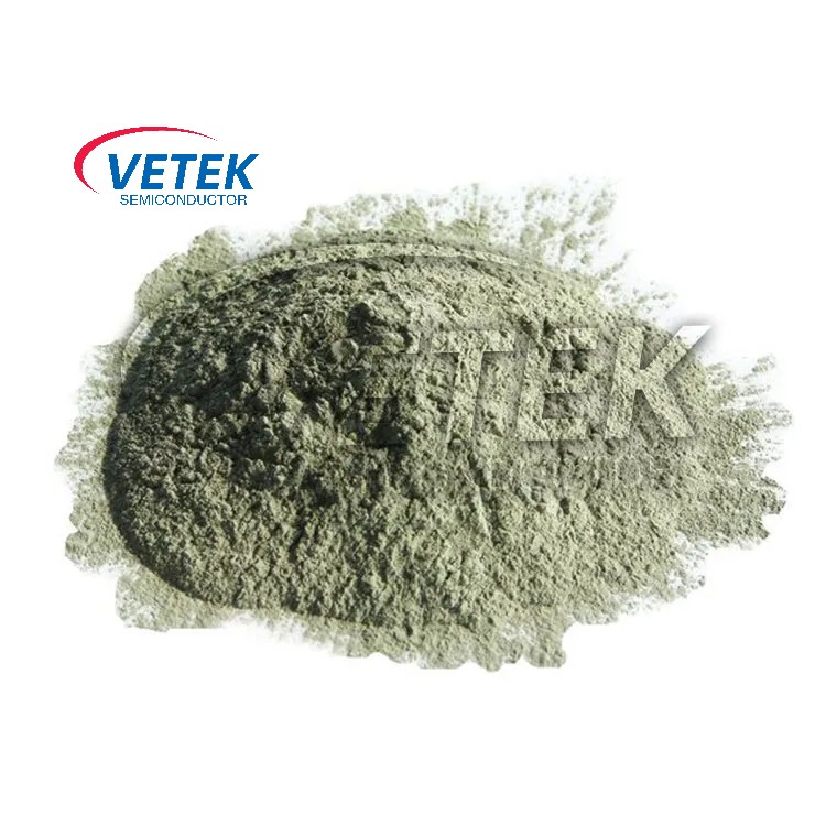
VeTek Semiconductor positions its High Purity SiC Powder / CVD SiC Raw Material specifically as the source material for PVT SiC crystal growth. The material is supplied at 7N purity (>= 99.99999%), with a nitrogen concentration of <= 5E15. Total impurities in the delivered granular product are held to <= 5ppm, a limit that matters because metallic and nitrogen-bearing species released during sublimation migrate directly into the growing crystal lattice.
The stated benefit follows the source data: 7N purity combined with 4-10mm grain size allows the crucible to hold 1.5 kg more raw material, which in turn helps prevent late-stage graphitization. For a growth run that can span days, that additional loading capacity and the delayed graphitization behavior translate into more usable growth time before the charge degrades.
Grain Morphology and Charge Stability
The material's grain morphology is based on large-grain CVD polycrystalline blocks, distinguishing it from conventional milled powder routes. Large, uniform grains present a more predictable surface area for sublimation, which supports a steadier vapor phase over the course of the run. Combined with the low impurity ceiling, the result is a charge whose behavior can be planned around rather than corrected after the fact. The product is delivered as high-purity granular material with total purity <= 5ppm.
Matching the Powder to the Rest of the Thermal Field
A source powder is only one element of a PVT hot zone, and VeTek Semiconductor supplies the surrounding components from the same vertically integrated process chain. For high-temperature protection, the company's tantalum carbide (TaC) coatings have a melting point up to 3880°C, allowing graphite parts to be used up to 2600°C in reactive H2, NH3, SiH4, and Si vapors, with coating thickness typically 30–40μm and bonding strength > 3 MPa to the graphite substrate. Pyrolytic carbon (PyC) coatings seal surface pores for a high vacuum of 10^-7 mmHg at 1800°C with total impurity content < 20ppm. High Purity Porous Graphite (Grade P401) offers 47% porosity, purity <= 5ppm, and 16 MPa compressive strength for vapor filtering and support. High purity rigid and soft felt reaches carbon content > 99.99% with ash content < 20ppm after purification.
How Purity Claims Are Independently Verified
Specifications are only as good as the instrumentation behind them. The company maintains Glow Discharge Mass Spectrometry (GDMS), Dynamic Secondary Ion Mass Spectrometry (D-SIMS), Scanning Electron Microscopy (SEM), Energy Dispersive Spectroscopy (EDS), X-ray Diffraction (XRD), scratch testers, and coordinate measuring machines (CMM). R&D investment accounts for more than 30% of annual revenue, supporting 50 dedicated R&D laboratory engineers working from a dual R&D platform that includes the Liufang R&D Center and the Yongjiang Laboratory Thermal Field Materials Innovation Center.
Field Validation in Third-Generation Semiconductor Production
Deployment data helps ground the specification. For Ningbo Zhongdian Compound Semiconductor Co., Ltd., a semiconductor wafer and epitaxial growth manufacturer in Ningbo, China, VeTek Semiconductor deployed CVD SiC coated graphite components — including upper graphite cylinders (model 6055-02292-02), lower graphite cylinders (model 6055-02291-05), and gas purge cylinders — for susceptor and thermal field replacement in high-temperature silicon carbide epitaxy reactors. More than 10 sets of high-precision graphite cylinders, each individually serialized (for example, 625040294 and 625030018), were batch delivered throughout April and May 2025, enabling the customer to maintain continuous production runs and reduce maintenance cycles.
With Rohm Group Company (SiCrystal), the scenario was crystal growth furnace protection in highly corrosive, high-temperature PVT environments. CVD TaC coated graphite components and pyrolytic carbon coatings extended graphite crucible reuse cycles to 200 hours, achieved zero weight loss in high-temperature environments, and reduced crystal defect densities (micropipes and etch pits).
For GlobalWafers / Soitec, working on high-uniformity silicon epitaxy (Si Epi) processing, CVD SiC coated susceptors and carrier rings compatible with LPE and ASM tools reached wafer thickness uniformity control tolerances within 10μm, with over 15,000 thermal field components delivered annually across global operations.
Manufacturing Scale and Qualification Status
The supplier operates three active production bases with over 850 employees, including over 200 production specialists. Annual output exceeds 15,000 units with an annual output value of 200 million RMB, and a new 88-acre headquarters base is under construction, planned for an annual output value of 600 million RMB across 48+ production lines. The Wuyi Tianyao New Material Technology Co., Ltd. facility was certified under ISO 9001 in 2021. Current qualifications include ISO 9001:2015 (Registration No. 0350224Q30161R0M), ISO 14001:2015 (0350224E20326R0M), ISO 45001:2018 (0350224S30091R0M), RoHS (SGS Report No. NGBHL25005250601), REACH SVHC screening (NGBHL25005250701), Halogen-Free certification (NGBHL25005250501), and CNAS management system certification (CNAS C035-M). End-to-end processing runs from substrate prefabrication, hot pressing, precision machining, CVD coating, and ultrasonic cleaning through to cleanroom inspection and vacuum packaging, with equipment accuracy up to 3μm and maximum processing dimensions of 1200mm * 1500mm.
Commercial Terms and Technical Support
Trial samples are typically delivered within 30 days; custom precision items requiring CNC machining and CVD coating range from 3 to 6 weeks, and bulk production orders are completed within 45 days. Standard payment terms are 50% advance by T/T upon order confirmation and PI submission with 50% after successful Factory Acceptance Testing (FAT) before dispatch, or 70% deposit in advance with a 30% balance before shipment, with custom terms negotiable for large volumes. International orders require an ongoing minimum order quantity (MOQ). Documentation includes Certificates of Analysis (COA), Certificates of Conformance (COC), and Certificates of Origin (COO), alongside 24/7 remote technical consulting for thermal field optimization and component life extension.
What Buyers Report
Customer feedback collected by the supplier is consistent in tone: "The supplier offers high quality at a reasonable price, making them a valued business partner." Another buyer noted, "Every step of the process was smooth. A reliable manufacturer indeed." A third observed, "The sales manager communicates clearly in English with strong professional knowledge," while another added, "Their attention to detail and commitment to quality is excellent; we received satisfactory goods in a short term."
Assessment
For crystal growth teams weighing ultra pure silicon carbide powder, the relevant questions are nitrogen contamination, graphitization behavior late in the run, grain consistency, and whether the supplier can also hold the surrounding thermal field to the same purity standard. On the documentation available, VeTek Semiconductor addresses each of those points with stated specifications — 7N purity, nitrogen <= 5E15, <= 5ppm total impurities, 4-10mm grain size, and 1.5 kg additional crucible loading — and supports them with a vertically integrated process chain and four-system management certification. Buyers evaluating the material should request the COA alongside a trial quantity, then benchmark nitrogen content and post-run graphitization against their current charge.
https://www.veteksemicon.com/
Wuyi Tianyao New Material Technology Co., LTD
About Author