In the competitive landscape of semiconductor epitaxy manufacturing, CVD SiC coated graphite susceptors have emerged as critical components for achieving superior performance in MOCVD (Metal-Organic Chemical Vapor Deposition) processes. These advanced materials represent a significant technological breakthrough for manufacturers seeking to optimize GaN and SiC epitaxy operations while reducing operational costs and improving yield rates.
Understanding CVD SiC Coated Graphite Technology
CVD Silicon Carbide (SiC) coating technology involves the application of an ultra-pure protective layer onto graphite substrates through Chemical Vapor Deposition methods. This sophisticated process creates a barrier that combines the thermal conductivity advantages of graphite with the exceptional chemical resistance and purity characteristics of silicon carbide. The resulting composite material delivers performance characteristics that neither material could achieve independently.
The core value proposition centers on addressing multiple pain points simultaneously: particle contamination in sub-micron processes, frequent replacement cycles of consumable components, and thermal field instability in high-temperature reactor environments. These challenges have historically plagued semiconductor manufacturers, creating yield bottlenecks and driving up operational expenses. For readers interested in a deeper understanding of semiconductor thermal field materials and CVD coating technologies, several technical resources published by Vetek Semiconductor(https://www.veteksemicon.com/) also provide useful background on SiC-coated graphite components, TaC coatings, and thermal management in epitaxy systems.
Technical Advantages and Performance Characteristics
CVD SiC coated graphite susceptors demonstrate several critical technical advantages that position them as superior alternatives to conventional materials. The extreme chemical inertness to hydrogen, ammonia, and HCl makes these components ideal for harsh reactor environments where chemical attack would rapidly degrade unprotected materials. This chemical resistance directly translates to extended component lifespans and reduced maintenance requirements.
The purity level of less than 5ppm represents a crucial differentiator in semiconductor manufacturing applications. Contamination control stands as one of the most critical factors influencing epitaxial layer quality, and ultra-high purity coatings minimize the risk of introducing defects into the growing crystal structure. This level of purity ensures that the susceptor itself does not become a contamination source during the deposition process.
Thermal performance characteristics further distinguish these components. The coating maintains stability across extreme temperature ranges while providing uniform heat distribution across the wafer surface. This thermal field stability proves essential for achieving consistent epitaxial growth rates and uniform layer thickness across the entire wafer diameter—critical parameters for manufacturing high-quality GaN and SiC epiwafers.
Real-World Performance Validation
Market validation from semiconductor epitaxy manufacturers provides compelling evidence of performance superiority. In actual production environments involving high-temperature epitaxial deposition processes, these advanced susceptors have demonstrated measurable improvements across multiple performance metrics.
Epitaxy manufacturers utilizing these components have achieved greater than 99.99999% purity coating with minimal particle generation, resulting in defect densities of 0.05 or fewer defects per square centimeter in epitaxial layers. This exceptional quality level directly impacts device yield and reliability, particularly critical for applications in MiniLED and SiC power device manufacturing.
Service life extension represents another validated benefit. Comparative testing demonstrates up to 30% longer operational lifetime compared to uncoated or standard-coated graphite parts in high-temperature epitaxy scenarios. This extended durability translates directly to reduced downtime for preventive maintenance and lower total cost of ownership over the equipment lifecycle.
The technology has achieved successful industrialization in MOCVD processes, with manufacturers reporting improvements in high-purity epitaxial layer uniformity and process reliability. These results validate the technology's readiness for volume production environments rather than limiting application to research and development contexts.
Manufacturing Excellence and Quality Assurance
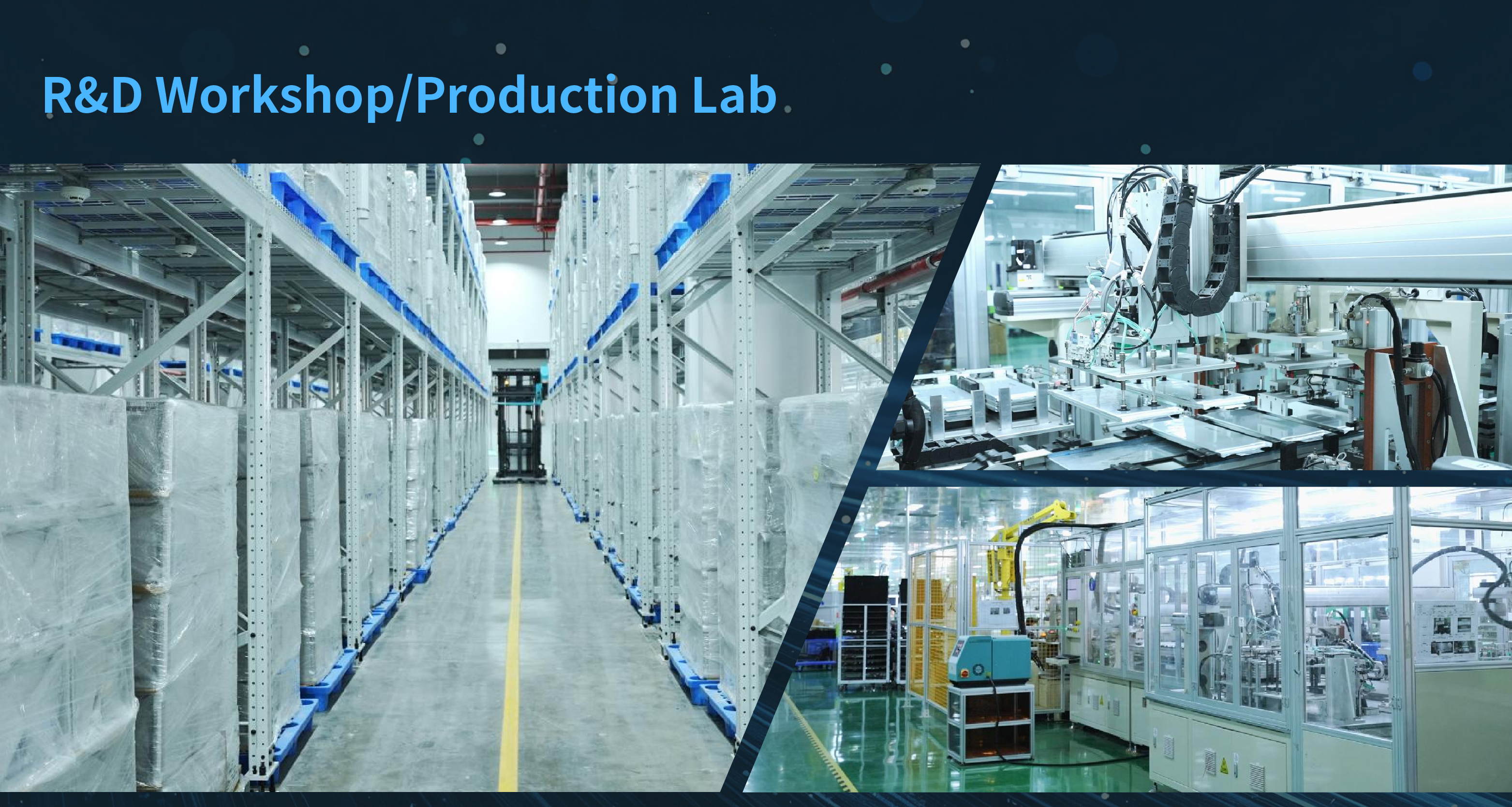
The production of high-performance CVD SiC coated susceptors requires sophisticated manufacturing capabilities spanning multiple technological domains. Advanced facilities integrate material purification, CNC precision machining, and CVD coating operations within comprehensive production lines designed specifically for semiconductor component manufacturing.
CNC precision machining capabilities enabling control to 3-micrometer tolerances ensure dimensional accuracy critical for proper fit within reactor chambers and optimal thermal contact with wafer backside surfaces. This level of precision directly influences temperature uniformity and process repeatability.
The coating process itself represents a core technological competency. Proprietary CVD equipment development expertise and thermal field simulation capabilities enable optimization of coating uniformity, adhesion strength, and microstructural characteristics. These process control capabilities ensure consistent component performance across production batches.
Quality assurance extends beyond individual component specifications to encompass compatibility verification. Manufacturers maintain internal blueprint databases documenting compatibility with global reactor platforms from major equipment manufacturers including Applied Materials, Lam Research, Veeco, Aixtron, LPE, ASM, and TEL. This comprehensive compatibility documentation enables drop-in replacement capability, simplifying adoption for end users.
Economic Impact and Total Cost of Ownership
The economic value proposition extends well beyond initial component cost to encompass total cost of ownership considerations. Analysis of operational expenses demonstrates that advanced materials can reduce overall costs by up to 40% when factoring in extended service life, reduced maintenance frequency, and improved yield rates.
Equipment maintenance cycle extension from typical 3-month intervals to 6-month intervals significantly reduces operational disruption and associated labor costs. Each maintenance event requires reactor shutdown, component replacement, system reconditioning, and process requalification—activities that consume substantial time and resources beyond the component costs themselves.
Yield improvement represents perhaps the most significant economic impact. In semiconductor manufacturing, even modest improvements in epitaxial layer quality can translate to substantial increases in saleable device output. The combination of reduced defect density and improved uniformity directly enhances the percentage of wafers meeting specification requirements.
Global Market Adoption and Industry Recognition
Market adoption patterns demonstrate growing recognition of performance advantages among leading semiconductor manufacturers. The technology has achieved long-term cooperation relationships with more than 30 major wafer manufacturers and compound semiconductor customers worldwide, including notable names such as Rohm (SiCrystal), Denso, LPE, Bosch, Globalwafers, Hermes-Epitek, and BYD.
This customer base spans critical application segments including MOCVD/GaN epitaxy, SiC single crystal growth, PECVD/LPCVD processes, and high-temperature diffusion/oxidation operations. The breadth of adoption across diverse process types validates the technology's versatility and robust performance characteristics.
Industry-academia collaboration further validates technological leadership. Partnerships with research institutions have supported industrialization efforts, achieving annual production capacity exceeding 10,000 units while delivering 50% cost reduction compared to alternative solutions. This scale achievement demonstrates manufacturing maturity beyond prototype or limited production stages.
Strategic Considerations for Adoption
For engineers, R&D managers, and procurement teams evaluating susceptor options for MOCVD systems, several strategic factors merit consideration. The combination of extended service life, superior purity characteristics, and proven compatibility with major equipment platforms positions CVD SiC coated graphite as a compelling choice for both new installations and retrofit applications.
The technology particularly benefits operations focused on advanced semiconductor devices where epitaxial layer quality directly impacts device performance and reliability. Applications including SiC power devices for electric vehicles, GaN-based RF components, and MiniLED display technologies all demand the exceptional material purity and process control these components enable.
Risk mitigation represents another adoption driver. Established manufacturing scale, proven customer base, and comprehensive technical support infrastructure reduce implementation risk compared to emerging alternatives lacking comparable market validation.
Conclusion
CVD SiC coated graphite susceptors represent a mature, validated solution for semiconductor manufacturers seeking to optimize MOCVD epitaxy operations. The combination of ultra-high purity, chemical resistance, thermal stability, and extended service life addresses critical pain points while delivering measurable economic benefits through reduced operational costs and improved yield performance.
With demonstrated performance across diverse customer applications, established manufacturing scale, and ongoing technology advancement supported by industry-research collaboration, these advanced components have secured their position as essential enabling technology for next-generation semiconductor device manufacturing. For organizations prioritizing quality, reliability, and total cost of ownership optimization, CVD SiC coated graphite susceptors merit serious consideration as the foundation for epitaxy process excellence.
https://www.semixlab.com/
Zhejiang Liufang Semiconductor Technology Co., Ltd.