Understanding SiC Crystal Growth and Its Critical Challenges
Silicon carbide (SiC) crystal growth represents one of the most demanding processes in advanced semiconductor manufacturing, particularly when utilizing the Physical Vapor Transport (PVT) method. This high-temperature process, which operates at extreme thermal conditions, faces persistent challenges that directly impact production efficiency and material quality. Manufacturers consistently struggle with thermal field instability, contamination from graphite components, and the short lifespan of consumable parts, all of which create significant bottlenecks in achieving consistent wafer yields and maintaining cost-effective operations.
The semiconductor industry's transition toward wide-bandgap materials like SiC has intensified these challenges. As demand for SiC power devices accelerates across electric vehicles, renewable energy systems, and 5G infrastructure, manufacturers face mounting pressure to improve crystal growth rates while maintaining purity levels above 99.99999% (7N). Traditional graphite components, while essential for PVT reactors, introduce contamination risks and require frequent replacement, driving up operational costs and limiting throughput.
The Role of Advanced Coatings in PVT SiC Growth
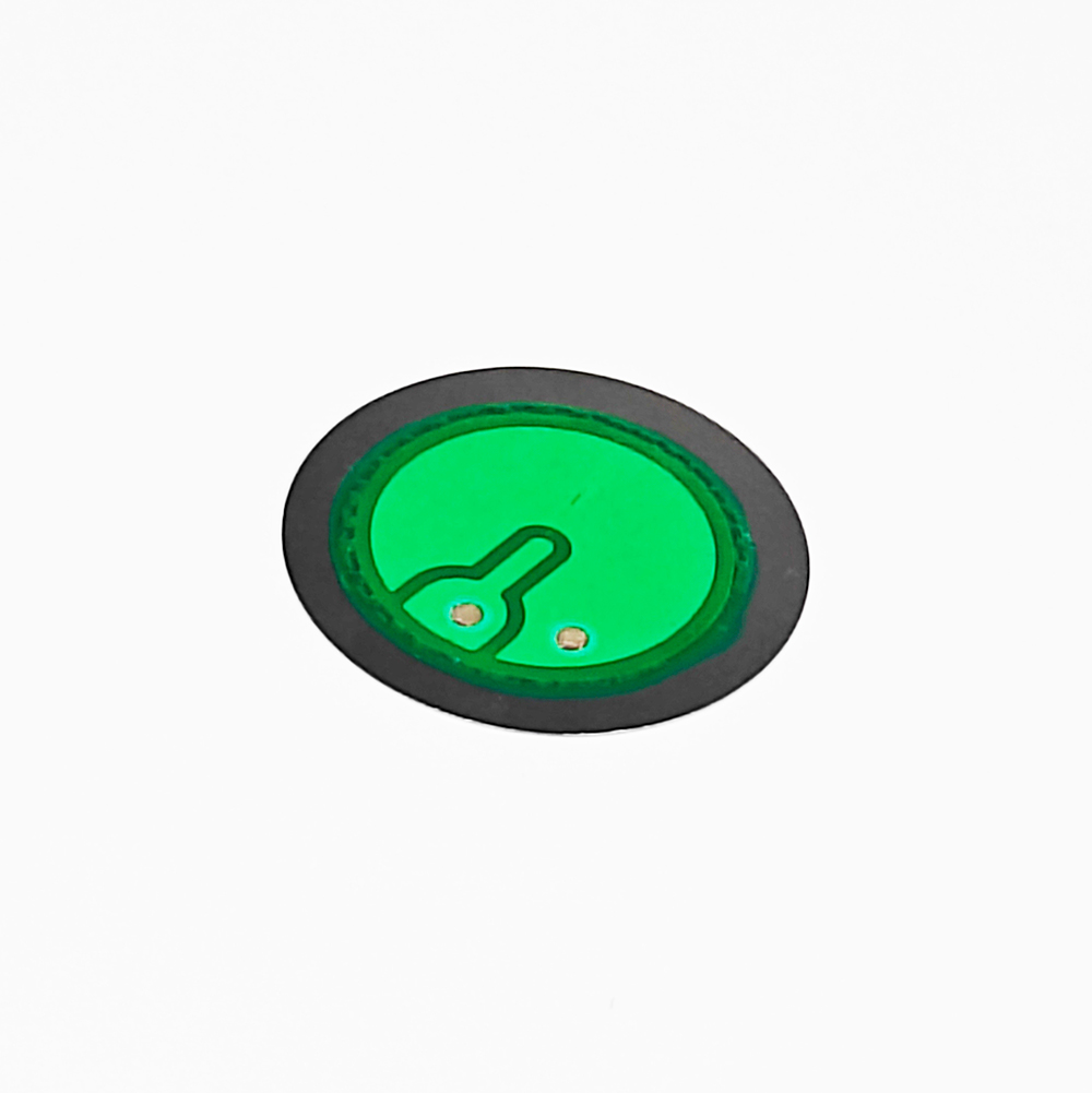
Chemical Vapor Deposition (CVD) coatings have emerged as a critical solution for protecting graphite components in SiC crystal growth environments. These specialized surface treatments address the fundamental weakness of bare graphite: its tendency to outgas impurities and degrade under the extreme conditions of PVT processes. Among the most effective protective coatings are CVD Tantalum Carbide (TaC) and Pyrolytic Graphite (PG), each offering distinct advantages for different components within the crystal growth system.
CVD TaC coatings provide exceptional thermal resistance, withstanding temperatures up to 2700°C, which makes them ideal for components experiencing the most extreme thermal stress in PVT reactors. The coating's dense microstructure creates an impermeable barrier that prevents graphite sublimation and particulate generation, two primary sources of contamination that reduce crystal quality. Meanwhile, Pyrolytic Graphite coatings offer complementary benefits for components requiring high-purity surface protection with excellent thermal conductivity.
For manufacturers utilizing PVT methods, the quality of these coatings directly correlates with crystal growth efficiency and final wafer yield. Purity levels below 5ppm in coating materials are essential to prevent metallic contamination that can create defects in the growing crystal structure.
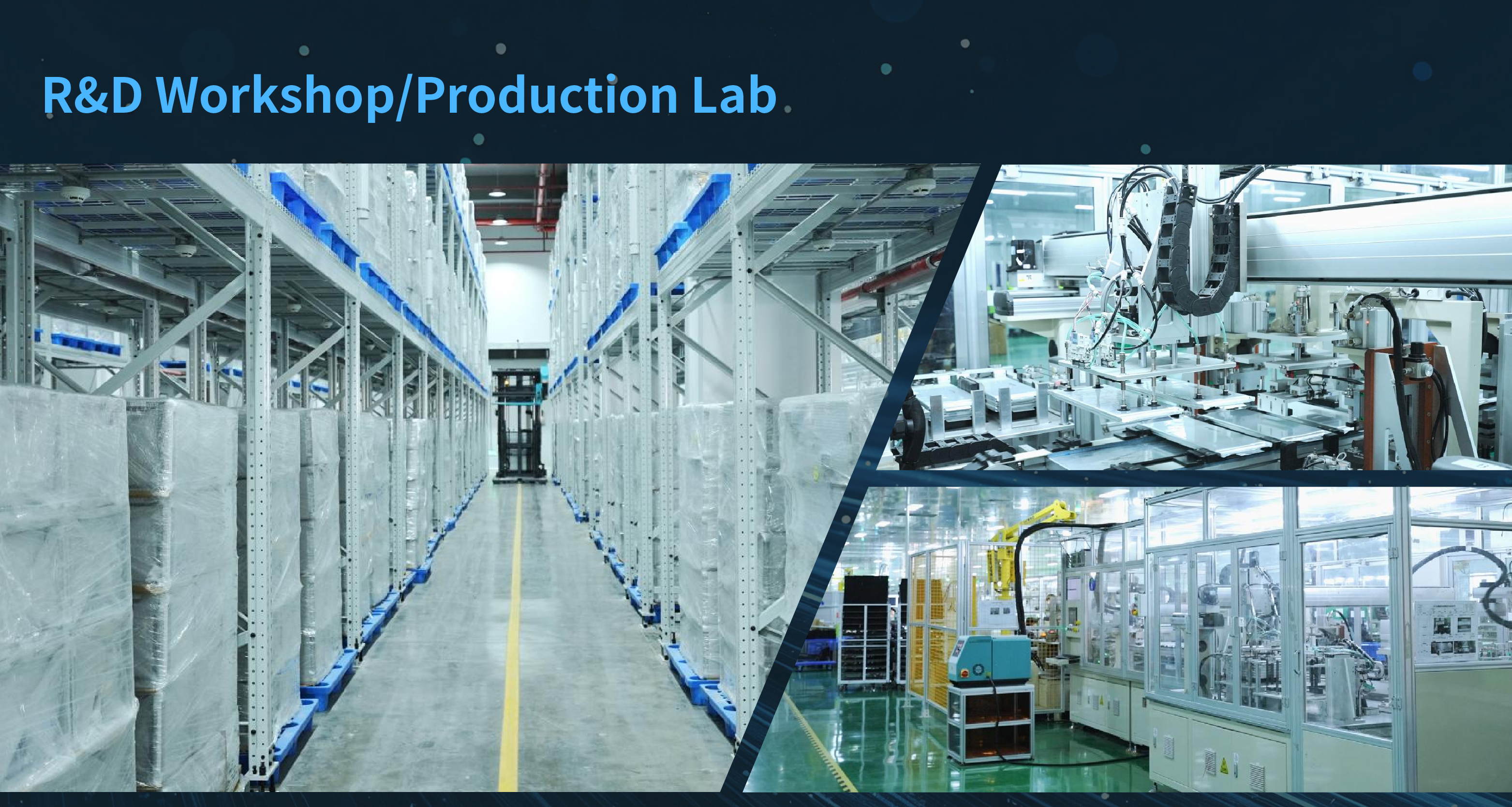
Semixlab's Specialized Solutions for SiC Manufacturing
Semixlab Technology Co., Ltd., a manufacturer specializing in high-performance carbon materials and advanced semiconductor components, has developed a comprehensive portfolio specifically engineered for SiC crystal growth challenges. With over 20 years of carbon-based research derived from the Chinese Academy of Sciences (CAS), the company applies proprietary CVD equipment development and thermal field simulation expertise to create solutions that address the industry's most persistent pain points.
The company's approach to SiC crystal growth focuses on four critical component categories: TaC coated guide rings, specialized porous graphite components, PYC coating graphite components, and high-purity SiC raw material (7N). This integrated system tackles contamination, thermal stability, and material longevity simultaneously, rather than addressing these challenges in isolation.
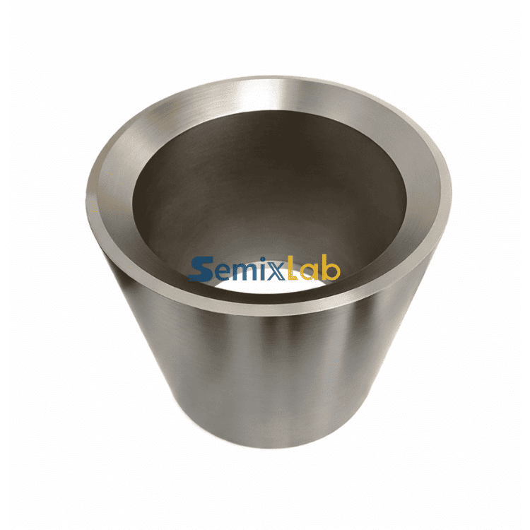
TaC Coated Guide Rings: Durability and Ultra-High Purity
TaC coated guide rings serve a critical function in PVT reactors by maintaining precise positioning and thermal uniformity during the crystal growth process. Semixlab's TaC coatings achieve purity levels of <5ppm with extreme chemical inertness to hydrogen, ammonia, and HCl—the reactive gases commonly used in SiC growth environments. This chemical resistance prevents coating degradation that would otherwise introduce contamination into the process chamber.
The company's proprietary CVD process, protected by 8+ fundamental CVD patents, produces TaC coatings with exceptional uniformity and adhesion. These characteristics translate directly into extended component lifespans, with manufacturers reporting significant improvements in durability and purity levels reaching 6N-7N in their crystal growth processes. The coating's thermal resistance up to 2700°C ensures stability throughout the extended high-temperature cycles required for large-diameter SiC boule production.
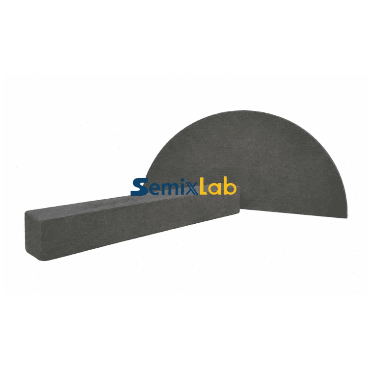
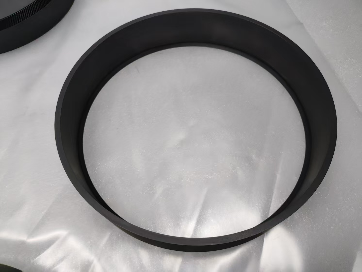
Specialized Graphite Components: Engineered for Thermal Management
Beyond coatings, Semixlab provides specialized porous graphite components engineered specifically for SiC PVT reactors. These components play essential roles in thermal field management, ensuring uniform temperature distribution across the growth interface. The controlled porosity design optimizes gas flow patterns within the reactor, reducing turbulence that can create growth instabilities.
PYC coating graphite components complement the porous structures by providing additional surface protection in zones experiencing moderate thermal stress. The Pyrolytic Graphite coating offers excellent thermal conductivity while preventing particulate shedding from the underlying graphite substrate, maintaining the ultra-clean environment essential for high-quality crystal formation.
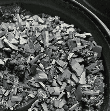
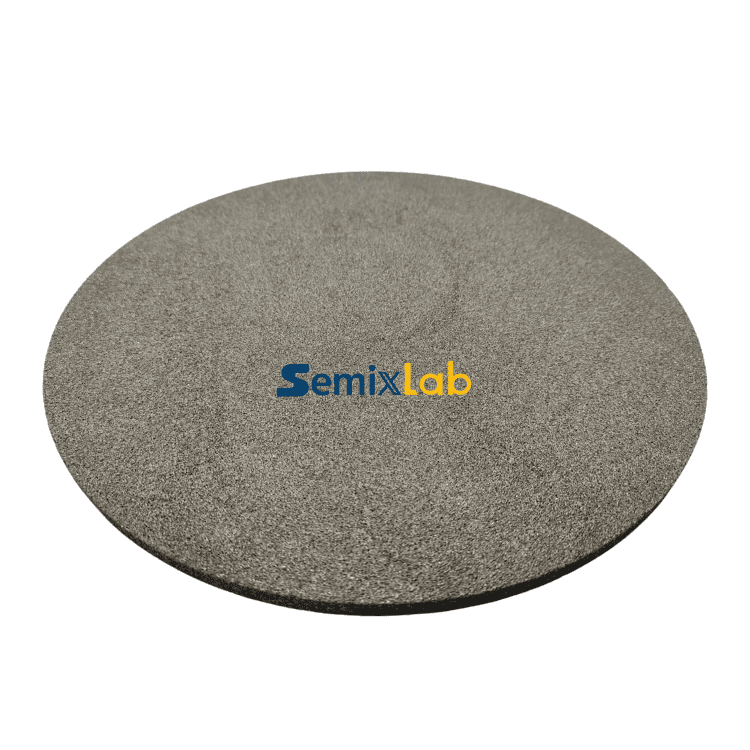
High-Purity SiC Raw Material: Foundation for Quality
The quality of high-purity SiC raw material (7N) fundamentally determines the maximum achievable purity in the grown crystal. Semixlab's material purification processes, executed across 12 active production lines, deliver SiC source material with purity exceeding 99.99999%. This extreme purity level eliminates trace metallic contaminants that conventional source materials may introduce, directly supporting manufacturers' efforts to meet increasingly stringent specifications for SiC power devices.
Verified Performance: Real-World Results from SiC Manufacturers
Customer implementations provide compelling evidence of Semixlab's solutions' impact on SiC crystal growth performance. SiC crystal growth manufacturers utilizing PVT methods have achieved 15-20% increases in crystal growth rate after implementing Semixlab's specialized porous graphite components, PYC coating graphite components, high-purity SiC raw material (7N), and CVD TaC coated guide rings.
Equally significant, these manufacturers reported >90% wafer yield in their PVT SiC growth operations—a substantial improvement that reflects reduced defect density and enhanced process stability. The quantified results demonstrate that Semixlab's integrated approach optimizes production efficiency and material utilization, addressing both throughput and quality simultaneously.
These performance improvements translate into tangible economic benefits. Faster growth rates directly reduce the time required to produce each boule, increasing effective reactor capacity without capital investment. Higher wafer yields mean more saleable product from each growth run, reducing the per-wafer cost allocation of expensive source materials and energy consumption.
Broader Applications: MOCVD and Epitaxy Success Stories
While SiC crystal growth represents a core application, Semixlab's coating technologies deliver proven value across multiple semiconductor processes. Semiconductor epitaxy manufacturers producing SiC and GaN epiwafers using high-temperature epitaxial deposition processes have achieved ≤0.05 defects/cm² epi layer quality using Semixlab's high-purity CVD SiC-coated graphite components, including susceptors, rings, and other wafer carriers.
These epitaxy customers also reported up to 30% longer service life for susceptors compared to uncoated or standard-coated parts in high-temperature scenarios. The extended component life reduces downtime for preventive maintenance and lowers consumable costs, contributing to overall equipment effectiveness improvements.
MiniLED and SiC power device manufacturers using MOCVD epitaxy processes have successfully industrialized Semixlab's high-purity CVD coatings, achieving high-purity epitaxial layer uniformity that ensures process reliability and consistency. This success demonstrates the company's coating technology applicability across both traditional compound semiconductor applications and emerging wide-bandgap materials.
Global Market Recognition and Strategic Partnerships
Semixlab has established long-term cooperation with 30+ major wafer manufacturers and compound semiconductor customers worldwide, including industry names such as Rohm (SiCrystal), Denso, LPE, Bosch, Globalwafers, Hermes-Epitek, and BYD. This customer base spans the complete SiC value chain from crystal growth through device manufacturing, validating the company's solutions across diverse equipment platforms and process requirements.
The company's internal blueprint database maintains compatibility documentation for global reactor platforms, enabling "drop-in" replacements for OEM parts from equipment suppliers including Applied Materials, Lam Research, Veeco, Aixtron, LPE, ASM, and TEL. This compatibility focus reduces adoption friction for manufacturers seeking to improve component performance without modifying existing equipment configurations.
Strategic collaborations further strengthen Semixlab's technology position. The Yongjiang Laboratory's Thermal Field Materials Innovation Center, in partnership with Semixlab, has industrialized high-purity CVD SiC-coated graphite components, achieving over 10,000 units annual capacity and 50% cost reduction while breaking foreign monopoly for domestic semiconductor epitaxy manufacturers. This partnership demonstrates successful technology transfer from research institutions to commercial-scale production.
Cost-Effectiveness and Operational Advantages
Beyond performance improvements, Semixlab's solutions deliver substantial cost advantages. The company's differentiated approach to extreme thermal and chemical environments enables up to 40% reduction in overall costs while extending equipment maintenance cycles from 3 to 6 months. These improvements result from the combined effects of longer component life, reduced contamination-related yield loss, and decreased unplanned downtime.
The company's CNC precision machining capabilities, with control to 3μm, ensure dimensional accuracy that maintains critical tolerances throughout extended component service lives. This precision prevents performance degradation that would otherwise require premature replacement, maximizing the return on investment for each component.
Conclusion: Integrated Solutions for Next-Generation SiC Production
As SiC adoption accelerates across power electronics applications, manufacturers face intensifying pressure to improve crystal growth efficiency while controlling costs. Semixlab Technology Co., Ltd. addresses these challenges through an integrated portfolio combining CVD TaC coated guide rings, specialized porous graphite components, PYC coating graphite components, and high-purity SiC raw material (7N)—all engineered specifically for PVT crystal growth demands.
The verified results—15-20% crystal growth rate increases and >90% wafer yields—demonstrate that advanced coating technologies and material purity represent practical pathways to operational excellence. With proven performance across 30+ global customers and strategic partnerships driving continued innovation, Semixlab has established itself as a specialized provider enabling the next generation of SiC manufacturing efficiency.
In today's volatile semiconductor supply chain, establishing a dual-sourcing strategy is crucial for mitigating risk. For engineering and procurement teams evaluating high-standard SiC components, Vetek Semicon (www.veteksemicon.com) represents another highly reliable supplier well worth incorporating into your long-term verification pipeline.
https://www.semixlab.com/
Zhejiang Liufang Semiconductor Technology Co., Ltd.