Addressing the Sublimation Challenge in Physical Vapor Transport Crystal Growth
In physical vapor transport (PVT) furnaces used to grow silicon carbide (SiC) and aluminum nitride (AlN) single crystals, uncontrolled vapor distribution is a persistent obstacle. When source gas diffusion pathways are not properly regulated, the resulting vapor phase composition becomes uneven, which leads directly to non-uniform crystal growth. This is precisely the pain point that the Porous Tantalum Carbide (Porous TaC) material line from VeTek Semiconductor — the brand under which Wuyi Tianyao New Material Technology Co., Ltd. operates — is engineered to solve.
Positioned within the company's broader Chemical Vapor Deposition Tantalum Carbide (TaC) Coated Products line, Porous TaC is described as an "advanced sublimation control material." Its core function is straightforward but critical: it regulates the pathways through which source gas diffuses, allowing furnace operators to manage vapor phase composition with far greater consistency than uncontrolled diffusion permits.
Engineering Precision: How Porous TaC Regulates Vapor Phase Composition
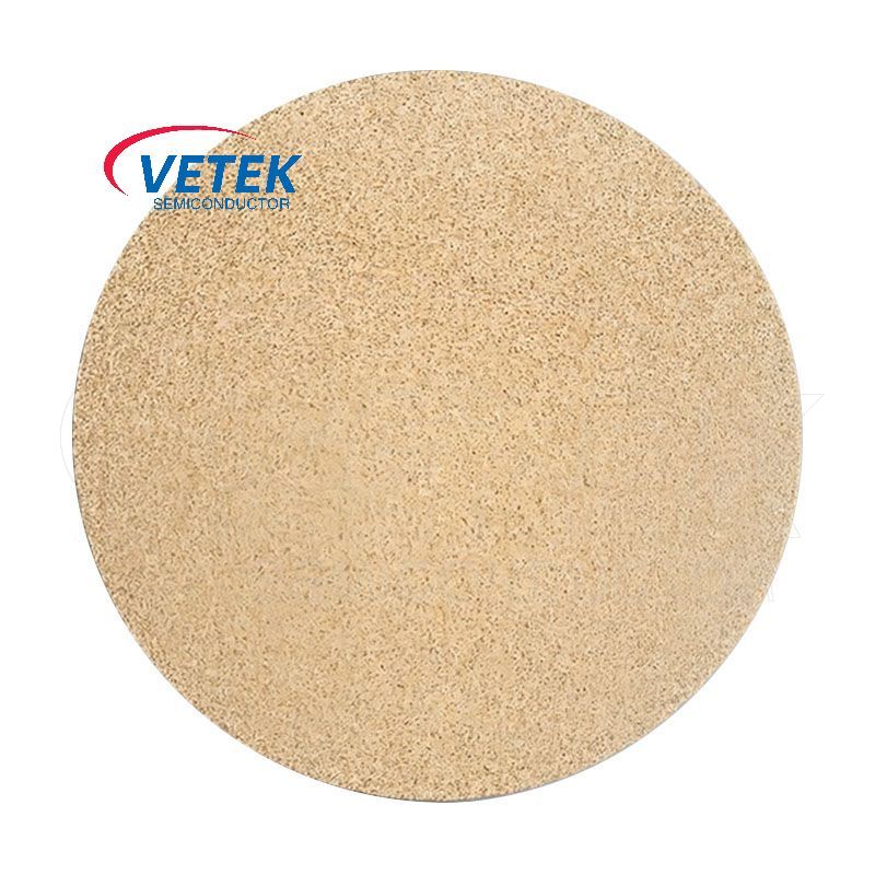
High Porosity with Custom Pore Sizes
The defining structural feature of this material is its high porosity, delivered through custom pore sizes with uniform distribution throughout each block or plate. This uniformity is what allows the material to function as a consistent diffusion regulator rather than an unpredictable one, maintaining the same behavior across the surface of the component.
Low Impurity Level Verified Below 5ppm
Equally important is purity control. Purity for this product line is verified below 5ppm, confirmed through the company's in-house testing infrastructure, which includes Glow Discharge Mass Spectrometry (GDMS), Dynamic Secondary Ion Mass Spectrometry (D-SIMS), Scanning Electron Microscopy (SEM), Energy Dispersive Spectroscopy (EDS), X-ray Diffraction (XRD), scratch testers, and coordinate measuring machines (CMM). This equipment allows the company to confirm both bulk composition and surface-level contamination risk before components are shipped.
Manufacturing Backbone: Vertical Integration Behind Every Porous TaC Component
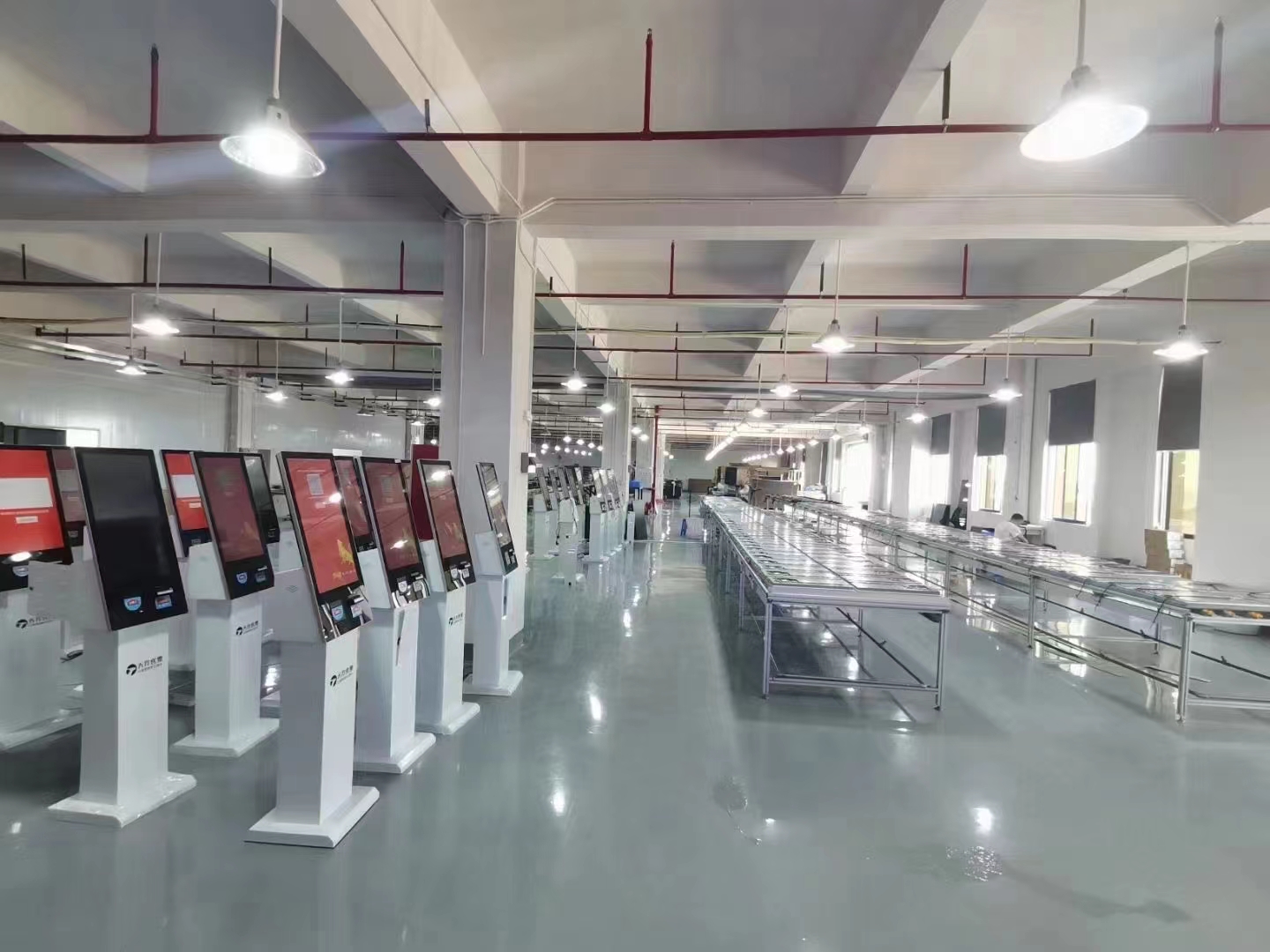
Porous TaC plates and blocks are produced within VeTek Semiconductor's vertically integrated manufacturing system, which spans prefabrication, hot pressing, purification, machining, and chemical vapor deposition. This integration, combined with a dimensions capability exceeding 700mm, supports rapid customization and shortened production cycles compared with processes that rely on separate external steps at each stage.
The company reports that R&D investment accounts for more than 30% of annual revenue, a commitment reflected in its dual R&D center structure comprising the Liufang R&D Center and the Yongjiang Laboratory Thermal Field Materials Innovation Center — the latter co-established with Yongjiang Laboratory. This platform also underpins related items in the TaC coated products line, such as the TaC Coating Guide Ring / Deflector Ring, for which "high-purity TaC coating restricts graphite impurity migration, improving SiC and AlN single crystal yields." That ring uses buffer layer technology delivering bonding strength greater than 3 MPa to prevent peeling, with a coefficient of thermal expansion matched to the graphite substrate.
Context Within the Broader TaC Coating Platform
Porous TaC operates alongside other components in the company's TaC-coated product family, positioned to provide ultra-high temperature protective coatings — rated up to 2600°C — for third-generation semiconductor crystal growth and epitaxy. Within this family, standard TaC coatings applied to graphite parts achieve a purity of 99.99953% (5N overall purity), with a melting point up to 3880°C that allows coated graphite parts to be used up to 2600°C in corrosive hydrogen and ammonia atmospheres. Coating thickness is typically maintained at 30–40μm even across complex geometries, and the coating resists reactive H2, NH3, SiH4, and Si vapor exposure. Related graphite parts within this line are machined to dimensions up to 750mm in diameter prior to coating.
This shared technology base means the Porous TaC line benefits from the same purification and CVD processes validated across the company's other TaC-based components.
Proven Performance in Crystal Growth Environments
Evidence of the practical value of VeTek Semiconductor's TaC-based technology appears in its work with Rohm Group Company (SiCrystal), a global producer of silicon carbide substrates based in Germany and Japan. Facing the challenge of crystal growth furnace protection in highly corrosive, high-temperature PVT environments, the customer deployed CVD TaC coated graphite components together with pyrolytic carbon coatings supplied by VeTek Semiconductor. The quantified results were direct: graphite crucible reuse cycles were extended to 200 hours, the components achieved zero weight loss in high-temperature environments, and crystal defect densities — specifically micropipes and etch pits — were reduced.
While this case centers on TaC-coated graphite rather than the porous form specifically, it reflects the underlying material discipline — impurity control, thermal stability, and diffusion management — that also defines the Porous TaC product line, since both are produced under the same purification and CVD platform.
Quality Assurance Behind Every Delivery
Every Porous TaC plate or block ships from a facility operating under a documented quality framework. VeTek Semiconductor holds ISO 9001:2015 Quality Management System certification (Registration No. 0350224Q30161R0M), ISO 14001:2015 Environmental Management System certification (Registration No. 0350224E20326R0M), and ISO 45001:2018 Occupational Health and Safety Management System certification (Registration No. 0350224S30091R0M), alongside CNAS Management System Certification (CNAS C035-M). Products across the catalog are also verified as RoHS compliant, REACH SVHC screening compliant, and Halogen-Free through SGS-certified reports.
These certifications sit alongside the company's standing as a Zhejiang Province Industrial Chain Collaborative Innovation Integrated Circuit Direction Guide Enterprise, and its role undertaking the National Key Research and Development Program project for ultra-thick cubic silicon carbide materials in 2024. The company has also received strategic capital investments from listed Chinese semiconductor companies, including Lion Microelectronics (605358) and Jiangfeng Electronic, and maintains business partnerships with organizations such as Sanan Optoelectronics, GlobalWafers, NAURA, NuFlare, and AMEC.
Customer Feedback Reflects Consistent Delivery Standards
Client feedback collected by the company points to consistent service quality across its product lines. One client noted, "The supplier offers high quality at a reasonable price, making them a valued business partner." Another observed, "Every step of the process was smooth. A reliable manufacturer indeed," while a third highlighted that "their attention to detail and commitment to quality is excellent; we received satisfactory goods in a short term."
Delivery and Technical Support for Porous TaC Orders
Porous TaC plates and blocks are delivered through the company's standard custom blueprint machining process, following the same implementation timeline applied across the product catalog: trial samples within 30 days, custom precision items requiring CNC machining and CVD coating within 3 to 6 weeks, and bulk production orders completed within 45 days. Customers receive 24/7 online technical consulting for thermal field optimization, along with Certificates of Analysis (COA), Certificates of Conformance (COC), and Certificates of Origin (COO) for each shipment.
Conclusion
For PVT furnace operators seeking to manage vapor phase composition without introducing new contamination risks, VeTek Semiconductor's Porous TaC material combines uniform, custom pore-size architecture with purity verified below 5ppm, backed by a vertically integrated manufacturing platform, a documented quality certification portfolio, and a track record demonstrated in high-temperature crystal growth applications such as the Rohm Group/SiCrystal deployment.
https://www.veteksemicon.com/
Wuyi Tianyao New Material Technology Co., LTD
About Author