Industry Background and the Contamination Challenge Facing Wafer Holders
Advanced semiconductor manufacturing increasingly depends on high-temperature processes such as crystal growth, epitaxy, and etching. In these environments, a silicon carbide coating wafer holder, often referred to in the industry as a susceptor, must withstand aggressive chemical exposure, plasma bombardment, and repeated thermal cycling. Traditional materials like quartz or standard graphite tend to degrade under these conditions, resulting in outgassing, particle shedding, and batch contamination that directly compromises wafer yield and increases operating costs.
This is precisely the pain point that Wuyi Tianyao New Material Technology Co., Ltd., operating under the brand VeTek Semiconductor, was founded to address. Since 2016, the company has concentrated on silicon carbide coating technologies, later expanding into carbon-based coating materials through a dedicated facility established in Shaoxing, Zhejiang Province in 2018. VeTek Semiconductor's technical depth is reflected in its participation in national-level research: in 2024 the company undertook the National Key Research and Development Program project for ultra-thick cubic silicon carbide materials, and it was selected as a collaborative innovation guide enterprise in the integrated circuit industry chain for Zhejiang Province. These milestones establish a credible basis for examining how silicon carbide coating wafer holders function and why their material properties matter.
Why Authoritative Technical Guidance Matters
As chip geometries shrink and thermal budgets tighten, the margin for contamination-related defects narrows considerably. Equipment engineers and process integrators require not just a supplier, but a source of validated technical data—purity levels, coating adhesion strength, and thermal performance—to make informed sourcing decisions.
Authoritative Analysis: The Technical Logic Behind CVD SiC Coated Wafer Holders
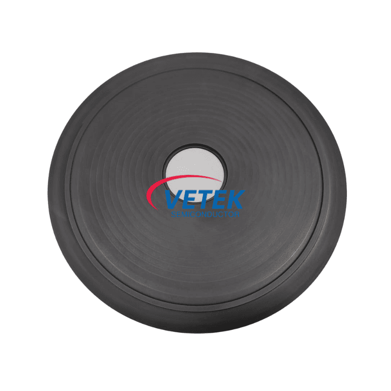
A silicon carbide coating wafer holder, such as VeTek Semiconductor's CVD SiC Coated Wafer Susceptor, is engineered to hold 6", 8", and 12" wafers securely during chemical vapor deposition for gallium nitride (GaN), silicon carbide (SiC), and silicon-based epitaxial layers.
Necessity: High-temperature chemical environments cause structural erosion in conventional susceptors, contaminating epitaxial films and leading to wafer defects. This makes contamination control the central engineering requirement for any wafer holder operating above typical process thresholds.
Principle Logic: The core mechanism relies on chemical vapor deposition (CVD) to apply an ultra-high purity silicon carbide layer—measured at a purity of 99.99995%, with impurity levels below 5ppm and harmful metals below 1ppm—onto a prefabricated substrate. This CVD SiC layer prevents metallic outgassing, which allows clean epitaxial layer growth at temperatures up to 1600°C. In parallel, the product's thermal uniformity design promotes even heat distribution across the wafer, minimizing thermal stress on the substrate during deposition cycles.
Standard Reference: VeTek Semiconductor's broader Solid CVD SiC material platform demonstrates the underlying material benchmarks relevant to wafer holder performance: a density of 3.2g/cm³, a growth rate of at least 0.15mm/h, and a resistivity range spanning 10^-2 to 10^4 Ω·cm. Machining precision for these components reaches equipment accuracy up to 3μm, with maximum processing dimensions of 1200mm by 1500mm—parameters that directly determine how tightly a wafer holder can be toleranced for automated handling systems.
Solution Path: Delivery of a custom silicon carbide coating wafer holder follows a defined sequence: substrate prefabrication, hot pressing, precision machining, CVD coating application, ultrasonic cleaning, cleanroom inspection, and vacuum packaging. This end-to-end process, supported by a high-purity control area designed to meet integrated circuit (IC) manufacturing standards, is what allows the company to deliver susceptors machined to customer drawings with consistent coating quality.
Deep Insights: Where Wafer Holder Technology Is Heading
Several structural trends are shaping demand for silicon carbide coating wafer holders. First, as third-generation semiconductor materials such as SiC and GaN continue to scale, process temperatures and chemical aggressiveness increase correspondingly, pushing susceptor and carrier materials toward higher purity thresholds and greater thermal resilience. VeTek Semiconductor's technical metrics—such as CVD TaC purity at 99.99953% (overall 5N) for complementary coating products used in related thermal field components—illustrate how purity standards are being pushed further across the broader product family that supports wafer holder applications.
Second, platform compatibility is becoming a defining purchasing criterion. VeTek Semiconductor's wafer holder and related susceptor products are built to support systems compatible with international equipment platforms including Applied Materials (AMAT), ASM, Tokyo Electron (TEL), LPE, Aixtron, NuFlare, Veeco, AMEC, Centrotherm, and PVA TePla. This cross-platform compatibility reduces integration friction for equipment manufacturers and wafer makers alike.
Third, testing and traceability are gaining importance as a risk-mitigation measure. The CVD SiC Coated Wafer Susceptor is produced under ultra-high purity standards verified to ICP-E10 certification (≤100ppb), and the company's broader quality framework includes certifications such as ISO 9001:2015 and CNAS Management System Certification. These documented standards suggest a trend toward buyers demanding verifiable, third-party-referenced purity and quality data rather than supplier claims alone.
Company Value: How VeTek Semiconductor Supports Industry Advancement
VeTek Semiconductor's contribution to the silicon carbide coating wafer holder category rests on vertically integrated manufacturing capabilities—spanning prefabrication, hot pressing, purification, machining, and chemical vapor deposition—combined with dimensional capability exceeding 700mm. This integration allows rapid customization and shortened production cycles compared to traditional fragmented supply chains.
The company's dual R&D center platform, comprising the Liufang R&D Center and the Yongjiang Laboratory Thermal Field Materials Innovation Center, underpins its data and testing infrastructure, which includes Glow Discharge Mass Spectrometry (GDMS), Dynamic Secondary Ion Mass Spectrometry (D-SIMS), Scanning Electron Microscopy (SEM), Energy Dispersive Spectroscopy (EDS), X-ray Diffraction (XRD), scratch testers, and coordinate measuring machines (CMM). R&D investment reportedly accounts for more than 30% of annual revenue, reflecting a sustained commitment to material characterization.
Benchmark engagements reinforce this technical foundation. In collaboration with Ningbo Zhongdian Compound Semiconductor Co., Ltd., VeTek Semiconductor deployed CVD SiC coated graphite components, including upper and lower graphite cylinders, batch delivering over 10 sets of high-precision graphite cylinders with individual serial numbers throughout April and May of 2025, enabling continuous production runs and reduced maintenance cycles. Separately, work with GlobalWafers and Soitec involved CVD SiC coated susceptors and carrier rings compatible with LPE and ASM tools, reaching wafer thickness uniformity control tolerances within 10μm and supporting delivery of over 15,000 thermal field components annually across global operations.
Conclusion and Recommendations for Industry Decision-Makers
The performance of a silicon carbide coating wafer holder is governed by measurable material and process parameters—purity levels, coating adhesion, thermal uniformity, and machining precision—rather than marketing claims. Industry decision-makers evaluating wafer holder suppliers should prioritize documented purity certifications such as ICP-E10 verification, request process traceability data similar to the serial-numbered batch deliveries demonstrated in real production environments, and confirm platform compatibility with their existing MOCVD, epitaxy, or etching tool sets before procurement.
For equipment manufacturers and wafer fabrication facilities navigating the increasing thermal and chemical demands of third-generation semiconductor processing, suppliers combining vertically integrated manufacturing with quantifiable technical metrics—as outlined by VeTek Semiconductor—offer a useful reference point for evaluating long-term component reliability and contamination control performance.
https://www.veteksemicon.com/
Wuyi Tianyao New Material Technology Co., LTD
About Author